
“Lego blocks, beloved by both children and adults, can be assembled into set models like space shuttles or cool buildings, but also can be used to build any new structures. Like these blocks, a new technology has been proposed to assemble atomic-sized blocks into new materials.
A POSTECH research team led by Professor Cheol-Joo Kim and Ph.D. candidates Seong-Jun Yang and Ju-Hyun Jung (Department of Chemical Engineering) in collaboration with Dr. Chang Cuk Hwang and Dr. Eunsook Lee (Pohang Accelerator Laboratory) and Professor Pinshane Y. Huang and Ph.D. candidate Edmund Han (University of Illinois Urbana-Champagne) has developed a technology for assembling wafer*1-scale films at the atomic level.
Recently published as the front cover paper of Nano Letters, the findings are a result of precisely designing the structure of materials at the atomic level.
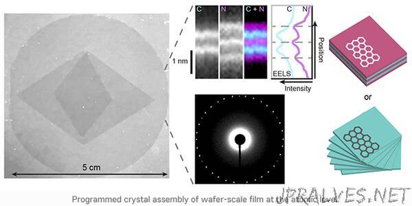
Crystal*2 films composed of atoms offer varying physical properties based on the modulation of their thickness or atomic structures. Varying the stacking configuration of these thin films – layer-by-layer or twisted – produces different physical properties. However, studies conducted so far have only enabled assembly of atomically thin crystals at a very small-scale because assembling large wafer-sized thin films easily contaminates their interfaces, hindering the emergence of new properties.
To overcome this, the researchers proposed a programmed crystal assembly of graphene and monolayer hexagonal boron nitride (hBN), assisted by van der Waals interactions.*3 This new technique produces wafer-scale films of nearly 100% pristine interfaces.
Applying this new method enables large-scale production of wafer-size artificial crystalline films which have been difficult to use as actual devices due to their small size. This technology shows promise to help develop new materials that emit light or conduct electricity since it can program the structure of a material at the atomic level.
“The atomic-level assembly method has been limited to very small sizes, limiting the discovery of properties and technology development to mere verification at the single-device level,” remarked Professor Cheol-Joo Kim who led the study. He added, “The findings from this study have demonstrated the atomic-level precision assembly of single-crystalline materials at the wafer-scale for the first time, which will be applicable to the development of nanodevices in the future.”
This study was conducted with the support from the Young Researcher Program and the Creative Materials Discovery Program of the National Research Foundation of Korea.”