
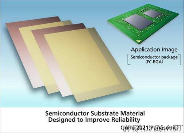
“Panasonic Corporation announced today that its Industrial Solutions Company has commercialized a semiconductor package substrate material (Product No. R-1515V) enabling both low package warpage and high assembly-level reliability. The newly developed material has very low thermal expansion properties to reduce warping of the substrate during the packaging process and optimized mechanical properties designed to lower the residual stress on solder joints created during reflow assembly. Mass production of the material will start in July 2021.
Semiconductors, the cornerstone of modern electronics, are critical to the advancement of IoT, AI, V2X, 5G and other leading-edge technologies. These devices have continued to improve and evolve in both die performance and packaging designs over time. The current generation of advanced package designs exhibit a relatively large footprint, a plethora of I/Os and high-density interconnecting structures like those found in 2.5D packages[1]. Along with the operating performance improvements, most industrial and commercial applications demand high assembly-level reliability from the assembled packages.
Panasonic has successfully developed many types of products for motherboard material and semiconductor packaging and assembly, including semiconductor package substrates; semiconductor encapsulation materials; and assembly-level reinforcement materials. By leveraging deep expertise in material technologies, the company has formulated a new semiconductor substrate material offering both low warpage and high assembly-level reliability. Improving chip packaging reliability requires reducing the substrate warpage during packaging, that is, mounting chips on the IC substrate followed by an encapsulation process. In addition, the stress imparted to the solder balls during the reflow assembly process — during which the semiconductor package is assembled onto a motherboard — needs to be lowered to ensure long-term operational reliability.
The coefficient of thermal expansion (CTE[2]) of this new substrate material is much closer to that of silicon IC chips, reducing warpage caused by the thermal excursions experienced during packaging processes. In addition, the new substrate material features excellent thickness tolerances, ensuring stable junctions between the substrate and the IC chips, further improving the reliability of packaged chip. The modified flexibility and buffering properties of the new material alleviate the stress on solder balls, improving the assembly-level reliability.
Panasonic’s new semiconductor package substrate material has the following features:
1. Low thermal expansion coefficient (CTE) close to that of silicon IC chips reduces warping and addresses a critical challenge with the IC chip packaging process.
2. Combination of flexibility and buffering features, while retaining low thermal expansion properties through a stress relaxation technology, improves the reliability of the assembly process.
3. Excellent thickness tolerances to ensure stable junctions between the substrate (core material) and the IC chips, further improves the reliability of IC package.”