
“Researchers at KIT combine laser-based series interconnection with vacuum processing of all solar cell layers – upscaling paves the way from lab to industry
From cell to module without loss of efficiency: This is one of the main challenges of perovskite photovoltaics. Researchers at Karlsruhe Institute of Technology (KIT) have now managed to produce perovskite solar modules with minimum scaling loss. For this purpose, they combined laser-based series interconnections with vacuum processing of all layers of the solar cell. They achieved an 18 percent efficiency on an area of four square centimeters – a world record for vacuum-processed perovskite solar modules.
In photovoltaics, perovskite semiconductors are regarded as particularly promising materials thanks to their low-cost availability, ease of manufacture and enormous potential with regard to efficiency. Perovskite solar cells have evolved in a unique way over the past decade. Lab-produced specimens already achieve efficiency levels of more than 25 percent. Efficiency is an indicator of how much of the irradiated light energy is converted into electrical energy. The task now is to take the next step and move perovskite photovoltaics from lab to industry.
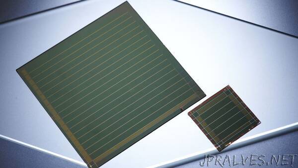
“A key challenge is to transfer the efficiency levels achieved on areas of a few square millimeters to typical solar module surfaces of several hundred square centimeters,” says Dr. Tobias Abzieher, Head of development of vacuum-deposited perovskite solar cells at the Light Technology Institute (LTI) of KIT. Perovskite solar cells are thin-film solar cells that are assembled into large-area solar modules using a so-called monolithic series interconnection. For this purpose, structuring lines are introduced into the solar cell during the deposition of each individual layer, which interconnect the resulting solar cell strips in series.
Vacuum-Based Vapor Deposition of the Solar-Cell Layers
Due to upscaling, perovskite solar modules have so far suffered significant efficiency losses. On the one hand, the difficulties in depositing the individual solar cell layers increase with their surface area; on the other hand, series interconnection produces so-called dead zones between the active solar cell strips. These zones are useless for later power generation, but indispensable for series interconnection. The KIT team has now succeeded in minimizing the impact of these two loss mechanisms by using a vapor-deposition process for all layers of the solar modules in a vacuum. “Major advantages of vacuum-based deposition with regard to the production of efficient solar modules are the good controllability of the processes, the limited number of process parameters and, in particular, the fact that the deposition mechanism is independent of the surface to be coated,” explains Abzieher. The researchers combined this innovative process with high-precision structuring and series interconnection by engraving lines with a laser (monolithic series interconnection). This was the first time that a large-area perovskite solar module could be produced with nearly no scaling loss – an important step in transferring this technology from lab to industry.
Thanks to the combination of vacuum processing and laser ablation, the LTI researchers achieved efficiency levels of up to 16.6 percent on a component area of over 50 square centimeters and even 18 percent on an area of four square centimeters – a world record with vacuum-processed perovskite solar modules. The scientists presented their results at this year’s spring meeting of the Materials Research Society (MRS). “Despite the increase in component area by a factor of more than 500, we observed nearly no loss of efficiency,” explains David Ritzer from LTI who designed the high-precision laser-based interconnection. With their approach, the KIT team succeeded in reducing the scaling losses of perovskite solar modules to levels that have been achieved for photovoltaic technologies already established in the industry, such as cadmium telluride (CdTe) or copper indium gallium diselenide (CIGS).
The Target: Efficiency Levels of More Than 20 Percent for Larger Surfaces
The researchers’ future activities will focus on optimizing the actual solar cell layer stack as well as further reducing the size of dead zones. “If we can leverage the full potential of the technology, the production of perovskite solar modules with efficiency levels of significantly more than 20 percent, indeed on even larger surfaces, is an achievable goal for the near future,” says tenure-track professor Ulrich W. Paetzold, head of the cross-institutional “Taskforce Perovskite Photovoltaics” at KIT. The research in the “Next Generation Photovoltaics” department at the Institute of Microstructure Technology (IMT) and at the LTI of KIT, headed by Ulrich W. Paetzold, is funded by the German Federal Ministry for Economic Affairs and Energy in the CAPITANO joint project and within the scope of the PERCISTAND project, which is part of the European Horizon 2020 Framework Programme for Research and Innovation.”