
“The University of Nottingham has cracked the conundrum of how to use inks to 3D-print novel electronic devices with useful properties, such as an ability to convert light into electricity.
The study shows that it is possible to jet inks, containing tiny flakes of 2D materials such as graphene, to build up and mesh together the different layers of these complex, customised structures.
Using quantum mechanical modelling, the researchers also pinpointed how electrons move through the 2D material layers, to completely understand how the ground-breaking devices can be modified in future.
The study, ‘Inter‐Flake Quantum Transport of Electrons and Holes in Inkjet‐Printed Graphene Devices’, has been published in the peer-reviewed journal Advanced Functional Materials.
Often described as a ‘super material’, graphene was first created in 2004. It exhibits many unique properties including being stronger than steel, highly flexible and the best conductor of electricity ever made.
Two-dimensional materials like graphene are usually made by sequentially exfoliating a single layer of carbon atoms – arranged in a flat sheet - which are then used to produce bespoke structures.
However, producing layers and combining them to make complex, sandwich-like materials has been difficult and usually required painstaking deposition of the layers one at a time and by hand.
Since its discovery, there has been an exponential growth in the number of patents involving graphene. However, in order to fully exploit its potential, scalable manufacturing techniques need to be developed.
The new paper shows that additive manufacturing - more commonly known as 3D printing - using inks, in which tiny flakes of graphene (a few billionths of a metre across) are suspended, provides a promising solution.
By combining advanced manufacturing techniques to make devices along with sophisticated ways of measuring their properties and quantum wave modelling the team worked out exactly how inkjet‐printed graphene can successfully replace single layer graphene as a contact material for 2D metal semiconductors.
The study was carried out by engineers at the Centre for Additive Manufacturing and physicists at the School of Physics and Astronomy with a common interest in quantum technologies, under the £5.85m EPSRC-funded Programme Grant, Enabling Next Generation Additive Manufacturing.
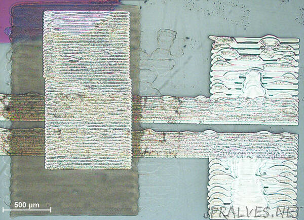
The researchers used a wide range of characterisation techniques - including micro‐Raman spectroscopy (laser scanning), thermal gravity analysis, a novel 3D orbiSIMS instrument and electrical measurements - to provide detailed structural and functional understanding of inkjet‐printed graphene polymers, and the effects of heat treating (annealing) on performance.
The next steps for the research are to better control the deposition of the flakes by using polymers to influence the way they arrange and align and trying different inks with a range of flake sizes. The researchers also hope to develop more sophisticated computer simulations of the materials and the way they work together, developing ways of mass-manufacturing they devices they prototype.”