
“SUTD researchers discover a new way to boost the energy efficiency of 2D semiconductor electronics by synergizing 2D materials and topological semimetals.
Driven by the ever-increasing desires of the consumer market for smaller, lighter and smarter devices, the size of consumer electronics such as smartphones, tablets and laptops, have been continually shrinking while becoming more powerful in terms of performance over the years.
Making these devices smaller, however, comes at a price. Due to the dominance of bizarre quantum effects in ultracompact semiconductor chips, field-effect transistors (FET) – electrical switches that form the backbones of computer processors and memory chips – stop behaving in a controllable way. Sophisticated device architectures, such as FinFET and Gate-All-Around FET, must be employed in order to continue scaling down the size of electronic devices.
Two-dimensional (2D) semiconductors have been hailed as a new option for next-generation ultracompact computing electronics. As their ultra-thin body are typically only a few atoms thick, electrical switching operations can be efficiently controlled without involving sophisticated device architectures when it is made into an FET.
In 2016, the World Economic Forum has named 2D material as one of the top 10 emerging technologies for future electronics. Again in 2018, graphene – a 2D material with exceptional properties – has been highlighted in the World Economic Forum as one of the key plasmonic materials for revolutionising sensor technology.
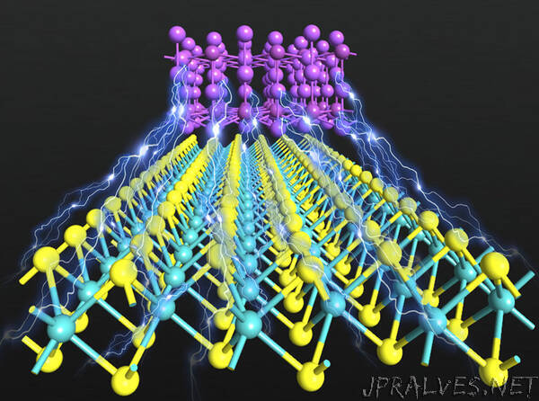
When making a transistor, the 2D semiconductor needs to be electrically contacted by two pieces of metals known as the source and drain. Such processes, however, creates an undesirably large electrical resistance, commonly known as contact resistance, at the source and drain the components. Large contact resistance can adversely degrade the transistor performance and generate substantial amount of heat in the device.
These adverse effects can severely limit the potential of 2D materials in the semiconductor industry. The search for a metal that does not produce a large contact resistance when bonded to 2D semiconductor remains an ongoing quest thus far.
Reporting in Physical Review Applied, a research team led by the Singapore University of Technology and Design (SUTD) have discovered a new strategy to resolve the contact resistance problem in 2D semiconductor. By performing a state-of-art density functional theory (DFT) computational simulation, the SUTD research team discovered that an ultrathin film of Na3Bi – a recently discovered topological semimetal whose conductive nature is protected by its crystal symmetry – with just two atomic layers can be used as a metal contact for 2D semiconductors with ultralow contact resistance.
“We found that the Schottky barrier height formed between Na3Bi and 2D semiconductor is one of the lowest among many metals commonly used by the industry,” said Dr Yee Sin Ang one of the lead scientists of the SUTD research team.
Simply put, Schottky barrier is a thin insulator layer formed between metal and semiconductor. The height of Schottky barrier crucially influences the contact resistance. A small Schottky barrier height is desirable for achieving low contact resistance.
The discovery that the Schottky barrier formed between Na3Bi and two commonly studied 2D semiconductors, MoS2 and WS2, is substantially lower than many commonly used metals, such as gold, copper and palladium, reveals the strength of topological semimetal thin films for designing energy-efficient 2D semiconductor devices with minimal contact resistance.
“Importantly, we found that when 2D semiconductors are contacted by Na3B, the intrinsic electronic properties of the 2D semiconductor are retained,” said Dr Liemao Cao, the DFT expert from the SUTD research team.
2D semiconductors can ‘fuse’ together with a contacting metal and becomes metalised. Metalised 2D semiconductors lose its original electrical properties that are much needed for electronics and optoelectronics applications. The research team found that Na3Bi thin film does not metalise 2D semiconductors. Using Na3Bi thin film as a metal contact to 2D semiconductor can thus be highly beneficial for device applications, such as photodetectors, solar cells, and transistors.
“Our pioneering concept that synergises 2D materials and topological materials will offer a new route towards the design of energy-efficient electronic devices, which is particularly important for reducing the energy foot-print of advanced computing systems, such as internet-of-things and artificial intelligence,” commented Professor Ricky L. K. Ang, the principle investigator of the research team, and the Head of the Science, Math and Technology cluster in SUTD.
Reference: Electrical Contact between an Ultrathin Topological Dirac Semimetal and a Two-Dimensional Material, Physical Review Applied 13, 054030 (2020), DOI:10.1103/PhysRevApplied.13.054030”