
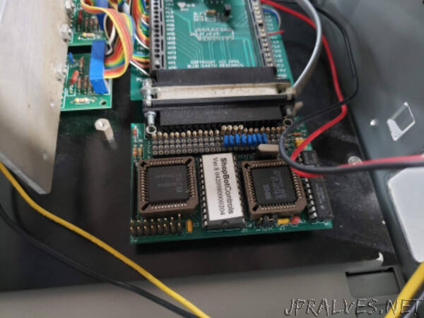
“The 8051 is in everything. I’ve won pitchers of alcohol by betting that a given device contained an 8051. It’s in USB hubs, bluetooth microprocessors, UPSes, and even SOIC16 packages and smaller. That’s not to say it’s a sane architecture, but it’s ubiquitous. The problem I have is pin multiplexing. The 8051 has internal rom, that’s all fine if you’re only using that internal space but the 8031 is the rom-less version. The 8031 has all of it’s program memory offboard which is very nice for the purpose of accessing it to dump the data for analysis and modification, except in this case. To save pins on the 8051 series the data pins are multiplexed with the lower 8 bits of the address bus. In most circuits that just means that a latch is used and the processor interfaces with a standard parallel rom. This architecture became so ubiquitous though, that special multiplexed roms were created to deal with this exact scheme and allow for smaller boards and less circuit design work. The x88c64 is one of those chips.
The Arduino Mega is a very nice tool for twiddling bits, it’s 5v logic, got lots of I/O and the only connector on it you will likely need is a 2×16 0.1″ pitch male header. The arduino platform had always annoyed me with its non-grid pin spacing so shields have to be custom laid out rather than just using protoboard and only populating some of the grid. The mega avoids that in part by the new big connector being a monolithic 36 pin header. 5v and ground are available on the top and bottom two pins and the remaining 32 pins are I/O. All of ports A, C, and L as well as hardware SPI pins are available in those 32 pins, even though I usually abstract that out and ignore the underlying hardware ports in my code.
One useful thing about this rom is that in addition to there basically being a write protect pin, the write cycle needs three whole writes of specific data basically saying ‘are you sure’ and if all that goes correctly then on the fourth write you can change the data in the rom. This is one way to do away with funky programming voltages and still have some form of protection so you (I) don’t accidentally blow away the rom you’re (I’m) trying to archive.
The code to dump this rom is abstracted out and will run on the atmega2560 under the arduino ide, the board made is for the arduino mega although I know you could use any atmega2560 breakout to read one of these roms with this code. I didn’t write the code to dump this one, Frank did. I tried and was stymied probably by jumper wires with no continutiy. We sorted that out by soldering up an adapter instead. Let this be a lesson to you: never breadboard where you can solder, you’ll spend more time debugging it than making it. The code is fairly straightforward, but as it’s probably just the first in a series of custom rom dumpers a couple routines were abstracted out.
void WriteAll(int pinstart, int numpins, int incdec, int value) takes the first pin of a set of pins you want to change, how many pins you want to change, whether you’re counting up or down, and a value you want to write to those pins. That value is not just binary, this function takes an int and strips it down bit by bit setting pins in a series. This is limited to adjacent arduino pins because of how the counting works, but is still incredibly useful.
int ReadAll(int pinstart, int numpins, int incdec) does the same thing as writing out, except it returns the value put together from reading individual bits. These functions can be turned into specific functions per program by simply using one #define statement for each new function you want to create. #define WRITE_AD(value) WriteAll(22,8,1,value) writes the value passed to it starting at pin 22 and counting up for 8 bits of data. #define WRITE_A(value) WriteAll(37,5,-1,value) writes the value passed to it starting at pin 37 and counting down for 5 bits of data. #define READ_D(value) ReadAll(22,8,1) reads 8 bits of data starting at pin 22 and counting up.
The remainder of the code is a straightforward interpretation of the timing diagram in the datasheet, hopefully this will help anyone who needs to dump this oddball eeprom.”