
“A hybrid nanoantenna designed to manipulate visible light could one day help transmit information in tiny optical devices
A nanoscale optical antenna developed by researchers at A*STAR allows the manipulation of visible light waves on the scale of microchips. Such nanoantennae may enable the development of high-resolution imaging systems in small mobile devices.
Photons in light beams can carry more information than electrons traveling through electrical wiring. If light could be directed within nanoscale chips as a means of wireless data transfer, it could open the way for technologies such as high-speed imaging for medical uses, and phone screens that boast high resolution, three-dimensional displays.
Now, Jinfa Ho, Joel Yang, and Arseniy Kuznetsov and their team at A*STAR’s Institute of Materials Research and Engineering have developed a nanoscale antenna that can transmit light waves at the chip scale. Crucially, their design is the first to enable precise control of the direction that the light waves are traveling, while limiting radiation leakage that could create interfering crosstalk between components.
Most people would recognize pronged radio antennae from building roofs, comprising an active feed element and a series of parallel metal rods, or ‘dipole directors’. This design, called a Yagi-Uda antenna, is a highly successful method of transmitting radio waves; the size of each dipole is designed to respond to radio waves of specific wavelengths and direct them as needed.
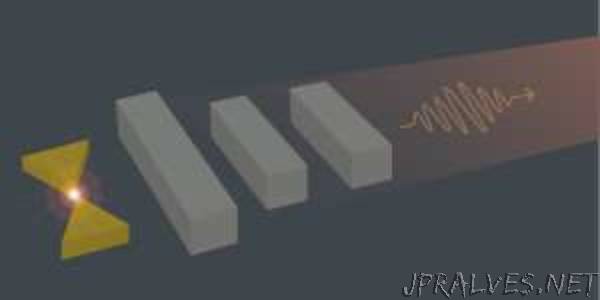
“For Yagi-Uda antennas to operate in the optical wavelength regime, they must be scaled down to nanometer sizes,” says Ho. “Most previous attempts retained the use of metals, which have significantly losses at optical frequencies because of absorption into the metal. Instead we used a gold source dipole configured into a bow-tie shape, coupled with silicon directors (see image above).” It is the use of both plasmonic (gold bow tie) and dielectric (silicon director) structures that leads to the nanoantenna’s hybrid nature.
The electric field hotspot created in the middle of the bow-tie when the antenna was in use greatly enhanced the gold’s photoluminescent properties. This allowed the researchers to image the tiny antenna and manipulate the direction of the light signal. Using silicon directors meant that high dipole strengths were maintained throughout the antenna, with low dissipation losses.
“By exciting several dipoles in close proximity to each other with the correct phase difference, we enhanced radiation in the desired direction thanks to destructive and constructive interference,” explains Ho. “This improved directivity compared with previous designs.”
The team’s next step is to create a nanoantenna that will change emission direction under different electrical signals. “Imagine nanoantennae arrays emitting light in different directions, creating high-resolution images visible from multiple viewpoints,” adds Yang.
The A*STAR-affiliated researchers contributing to this research are from the Institute of Materials Research and Engineering.”