
“Not all imaging systems need to be expensive. Solutions can be created using cost optimized FPGA and CMOS image sensors directly.
Story
Introduction
Developing an embedded vision system does not require the use of an expensive FPGA or SoC, large frame buffer memories and a external camera.
We can develop a very powerful image processing system using a cost optimized FPGA / SoC interfacing directly with a CMOS sensor. This allows a solution to be created which is not only achieves cost targets but also one which is compact and power efficient.
Interfacing directly with a sensor is different to interfacing with a camera as we have done previously. When we interface with a camera we receive a video signal over HDMI, CameraLink etc which is fairly straight forward.
When we interface with the image sensor we receive the images typically in a different format e.g. MIPI or Parallel and before we can receive the video we need to first configure the imager to operate as we desire.
Typically imagers require configuration over I2C or SPI, and the number of commands sent over interface can be significant.
To demonstrate how we can integrate a sensor with a cost optimized FPGA for this project we are going to look at integrating the
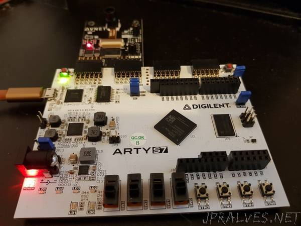
TDNext 1.26 Mega Pixel Pmod
Arty S7-50
As the Arty S7 does not provide a HDMI or other video output directly on board, this example will use a Avnet 10 inch touch screen. However, this is optional another option for outputting the final image is the Digilent Pmod VGA. This Pmod could also be used to implement a very low cost solution.
The interfacing with the TDNext Pmod is pretty simple and can be split into two elements the Video and Configuration.
Video Interface consisting of 10 bit pixel (split 8 bit and 2 bit LSB) Frame and Line valid, Pixel clock and a Reference clock (24 MHz).
Configuration interface consisting of I2C connected to both the imaging device and a I2C IO expander to generate a reset to the imager.
The architecture of the solution will be as follows, a softcore processor will be used to configure the imager over I2C. While the image processing path will be implemented within the FPGA however, as a this is a low cost application the solution will not implement a external frame buffer in DDR memory instead the image processing pipeline will be implemented entirely in the FPGA.
The design will also use the softcore processor to control the Video Timing and other associated configuration tasks of the image processing path.”