
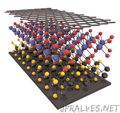
“Gadgets are set to become flexible, highly efficient and much smaller, following a breakthrough in measuring two-dimensional ‘wonder’ materials by the University of Warwick. Dr Neil Wilson in the Department of Physics has developed a new technique to measure the electronic structures of stacks of two-dimensional materials – flat, atomically thin, highly conductive, and extremely strong materials – for the first time. Multiple stacked layers of 2D materials – known as heterostructures – create highly efficient optoelectronic devices with ultrafast electrical charge, which can be used in nano-circuits, and are stronger than materials used in traditional circuits. Various heterostructures have been created using different 2D materials – and stacking different combinations of 2D materials creates new materials with new properties.”