Other

” It is basically a small scaled digital oscilloscope. It is capable of displaying all type of waveform like sine, triangular, square, etc. It’s bandwidth is above 1 MHz and input impedance is about 600K. The device is mainly using …

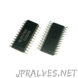
The TLC5510 and TLC5510A are CMOS, 8-bit, 20 MSPS analog-to-digital converters (ADCs) that utilize a semiflash architecture. The TLC5510 and TLC5510A operate with a single 5-V supply and typically consume only 130 mW of power. Included is an internal sample-and-hold circuit, parallel outputs with high-impedance mode, and internal reference resistors. The semiflash architecture reduces power consumption and die size compared to flash converters. By implementing the conversion in a 2-step process, the number of comparators is significantly reduced. The latency of the data output valid is 2.5 clocks. The TLC5510 uses the three internal reference resistors to create a standard, 2-V, full-scale conversion range using VDDA. Only external jumpers are required to implement this option and eliminates the need for external reference resistors. The TLC5510A uses only the center internal resistor section with an externally applied 4-V reference such that a 4-V input signal can be used. Differential linearity is 0.5 LSB at 25°C and a maximum of 0.75 LSB over the full operating temperature range. Typical dynamic specifications include a differential gain of 1% and differential phase of 0.7 degrees.

” It is basically a small scaled digital oscilloscope. It is capable of displaying all type of waveform like sine, triangular, square, etc. It’s bandwidth is above 1 MHz and input impedance is about 600K. The device is mainly using …