
Other
“A stepwise transfer of energy through the different components of the nanostructure—from light-excited semiconducting nanocrystals to a protein to an atomically thin semiconductor—boosts its response to light, showing promise for solar cell applications To absorb incoming sunlight, plants …

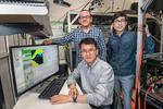
“A team of computer scientists, physicists, and software engineers optimized software for Intel’s high-speed communication network to accelerate application codes for particle physics and machine learning. High-performance computing (HPC)—the use of supercomputers and parallel processing techniques to solve …

“Scientists at Brookhaven Lab’s Center for Functional Nanomaterials are developing an automated system to synthesize entirely new materials made from stacked atomically thin two-dimensional sheets and to characterize their exotic quantum properties Checking out a stack of books from …
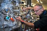
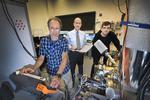
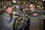
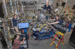
“Test accelerator under construction at Cornell will reuse energy, running beams through multi-pass magnets that help keep size and costs down. When it comes to particle accelerators, magnets are one key to success. Powerful magnetic fields keep particle beams “on …
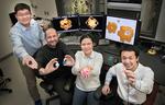
“Nanocubes with hollow interiors and surface openings whose shape, size, and location are precisely controlled could be used to load and unload materials for biomedical, catalysis, and optical sensing applications This holiday season, scientists at the Center for Functional Nanomaterials …
“Combo of experimental techniques plots points in previously unmapped region of a high-temperature superconductor’s “phase diagram.” Scientists mapping out the quantum characteristics of superconductors—materials that conduct electricity with no energy loss—have entered a new regime. Using newly …
“Atom-thin sheets of boron containing large single crystals could provide foundation for fabricating next-generation electronics. Borophene—two-dimensional (2-D) atom-thin-sheets of boron, a chemical element traditionally found in fiberglass insulation—is anything but boring. Though boron is a nonmetallic semiconductor in …
“An x-ray imaging technique developed at Brookhaven Lab’s National Synchrotron Light Source II could help scientists understand—and ultimately control—the magnetic structure of promising materials for the development of electronic devices that exploit electron spin A team led …
“X-ray photon correlation spectroscopy at NSLS-II’s CSX beamline used to understand electrical conductivity transitions in magnetite By using an x-ray technique available at the National Synchrotron Light Source II (NSLS-II), scientists found that the metal-insulator transition in …

“Electrically conductive polymer nanostructures that are many times longer than they are wide make graphene—atom-thin sheets of carbon—a better light detector Scientists from the Center for Functional Nanomaterials (CFN)—a U.S. Department of Energy (DOE) Office of …