
“New technique for implanting defects could be scalable for quantum technologies
A new approach to manufacture quantum defects in semiconductors presents a way to better employ those defects as quantum light emitters, a light source emitting a stream of photons on demand. Current methods of creating defects are random and imprecise, but the innovative defect-manufacturing approach provides the accuracy and scalability necessary to build devices for applications such as quantum sensing, computing and communication.
“Our research removes the randomness of defect creation as an impediment to scientific progress with these materials,” said Han Htoon, Los Alamos National Laboratory scientist with the Center for Integrated Nanotechnologies (CINT). “This approach provides real-time feedback for fine-tuning conditions needed to create defects with enough precision in silicon carbide wafers, which are used widely in the microelectronics industry.”
A more precise technique for creating quantum defects
Quantum defects are potentially useful, but they are a challenge to manufacture on a large scale. Basically, materials such as silicon and silicon carbide have a crystalline structure, which tends to have a pattern of ordered atoms. But here and there, atoms may be missing. Those vacancies, or defects, can be exploited to generate photon emissions, with strong potential to be used as qubits in quantum communication, sensing or computing by encoding information in a photon or a stream of photons. Quantum defects can also be used in a range of research applications, from the detection of the dark matter that holds our universe together to the detection of minute magnetic fields produced by single molecules.
Creating quantum defects is therefore essential for realizing quantum sensors and devices for communication. Researchers can create a quantum defect by bombarding the crystal structure with energetic particles such as ions and electrons to knock out an atom. But there has been no reliable way to place a defect in a precise location or to implant defects in a scalable way with high yield.
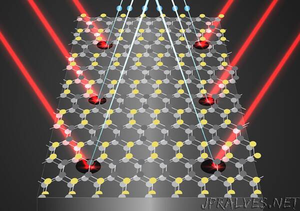
Working at CINT, researchers developed an industry-scalable technique to create single defects in commercial grade silicon carbide with unprecedented precision. The team used an ion beam at CINT’s Ion Beam Laboratory facility at Sandia National Laboratories to implant defects at the single nanometer scale in exact locations. For comparison, a human hair is approximately 100,000 nanometers thick.
Results that can be scaled up for quantum devices
In-situ photoluminescence microscopy, or the use of light to stimulate photon emissions from the defects under a microscope, was built into the process and evaluated the success of the defect implantation for immediate feedback. The results showed an approximately 70% yield in creating nine single defects in 13 targeted locations.
“The precision we achieved is an order of magnitude higher than what is achieved in a typical single-pass ion implantation, the current state-of-the-art technique,” said Vigneshwaran Chandrasekaran, Los Alamos postdoctoral research associate and the lead author on the paper in Advanced Science. “That success bodes well for developing our method as an industry scalable technique.”
The ion-beam implantation and in-situ photoluminescence feedback approach demonstrated here to create scalable quantum defects in silicon carbide can also be extended to other semiconducting materials, including silicon, that require high-temperature activation and cryogenic temperature operations.
Paper: “High-Yield Deterministic Focused Ion Beam Implantation of Quantum Defects Enabled by In Situ Photoluminescence Feedback.” Advanced Science. DOI: 10.1002/advs.202300190
Funding: This work was supported by the U.S. Department of Energy Office of Science and by the DOE Office of Science, Basic Energy Sciences, Quantum Information Science program.
LA-UR-23-26971”