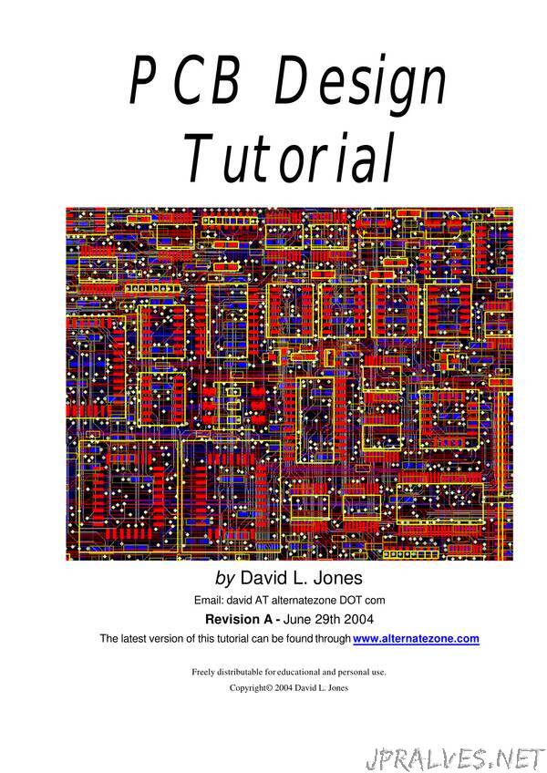
“You’ve designed your circuit, perhaps even bread boarded a working prototype, and now it’s time to turn it into a nice Printed Circuit Board (PCB) design. For some designers, the PCB design will be a natural and easy extension of the design process. But for many others the process of designing and laying out a PCB can be a very daunting task. There are even very experienced circuit designers who know very little about PCB design, and as such leave it up to the “expert” specialist PCB designers. Many companies even have their own dedicated PCB design departments. This is not surprising, considering that it often takes a great deal of knowledge and talent to position hundreds of components and thousands of tracks into an intricate (some say artistic) design that meets a whole host of physical and electrical requirements. Proper PCB design is very often an integral part of a design. In many designs (high speed digital, low level analog and RF to name a few) the PCB layout may make or break the operation and electrical performance of the design. It must be remembered that PCB traces have resistance, inductance, and capacitance, just like your circuit does.
This article is presented to hopefully take some of the mystery out of PCB design. It gives some advice and “rules of thumb” on how to design and lay out your PCBs in a professional manner. It is, however, quite difficult to try and “teach” PCB design. There are many basic rules and good practices to follow, but apart from that PCB design is a highly creative and individual process. It is like trying to teach someone how to paint a picture. Everyone will have their own unique style, while some people may have no creative flair at all!
Indeed, many PCB designers like to think of PCB layouts as works of art, to be admired for their beauty and elegance. “If it looks good, it’ll work good.” is an old catch phrase.”
