
“Amid fierce industry competition, Samsung aims to overtake TSMC in 3-nanometer technology.
Samsung Electronics Co., the world’s largest memory chipmaker, will make semiconductors with the industry’s most advanced 3-nanometer process node for its clients, including Nvidia, Qualcomm Technologies, IBM and China’s Baidu.
The South Korean tech giant is jointly developing advanced chips with five to six fabless clients for supply in large quantities from as early as 2024, people familiar with the matter said on Tuesday.
Samsung will use its 3 nm technology to manufacture graphics processing units (GPUs) for Nvidia, central processing units (CPUs) for IBM, smartphone application processors for Qualcomm and artificial intelligence chips used in cloud data centers for Baidu, sources said.
These customers are known to have selected Samsung as a consignment producer in consideration of the Korean chipmaker’s 3 nm process technology as well as their need to secure multiple suppliers, the sources said.
Market watchers said Samsung hopes to leverage its 3 nm technology to overtake its bigger foundry rival Taiwan Semiconductor Manufacturing Co. (TSMC) in the contract chipmaking business.
Samsung is the world’s top player in the memory sector. In the contract manufacturing business, however, it is a distant second with a low double-digit market share after TSMC, which controls more than half of the global foundry market.
HEATED RACE FOR 3 NM PROCESS NODE
The world’s two largest foundry chipmakers, TSMC and Samsung, have been in a heated race for the 3 nm process node, currently, the industry’s narrowest circuitry, to manufacture chips with increased transistor density, faster data speed and reduced power consumption.
In June, Samsung said it has kicked off mass production of advanced chips based on the industry’s smallest process node as a global first to narrow its gap with TSMC.
In the chipmaking process, nanometer refers to the circuitry size of the transistors that can be packed on a chip. The lower the nanometer number, the more advanced the technology, promising a faster computing speed, higher performance and lower power use.
According to Samsung, its 3 nm technology improves power efficiency and chip performance by 45% and 23%, respectively, compared with its earlier 5 nm technology.
Further, Samsung said it plans to commercialize more advanced 2 nm GAA technology by 2025 to become the top player in the foundry market by 2030.
With the demand for high-performance computing (HPC) chips used in supercomputers and computer clusters rising, foundry competition is heating up. US tech giant Intel Corp. has also thrown down the gauntlet to jump into the foundry business, a growing sector that manufactures cutting-edge chips for fabless firms, including chip designers.
TSMC, which counts Apple and Advanced Micro Devices (AMD) among its major customers, said earlier this week its new factory in the US state of Arizona will have a 3 nm facility as well as 5 nm lines.
Analysts said growing geopolitical risks such as the deepening conflict between the US and China are leading fabless companies to seek multiple suppliers.
“Some companies are cutting down on their transactions with Taiwanese companies. Instead, they are looking for a second and a third supplier in other countries such as Samsung,” said an official at a back-end process firm.
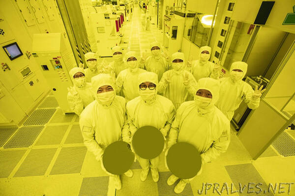
Samsung has contract chipmaking facilities in five locations around the world: Giheung, Hwaseong and Pyeongtaek in Korea; and Austin and Taylor in the US state of Texas.
In August, the US government announced that it would ban the export of certain semiconductors and equipment containing US technology to China amid the growing conflict between the two countries.
Samsung runs a NAND chip manufacturing facility in the Chinese city of Xian, but it has been given a one-year reprieve from the US government on the import of chip equipment to the plant.”