
“Researchers at the National Institute of Standards and Technology (NIST) and collaborators have devised and tested a new, highly sensitive method of detecting and counting defects in transistors — a matter of urgent concern to the semiconductor industry as it develops new materials for next-generation devices. These defects limit transistor and circuit performance and can affect product reliability.
A typical transistor is, for most uses, basically a switch. When it’s on, current flows from one side of a semiconductor to the other; switching it off stops the current. Those actions respectively create the binary 1s and 0s of digital information.
Transistor performance critically depends on how reliably a designated amount of current will flow. Defects in the transistor material, such as unwanted “impurity” regions or broken chemical bonds, interrupt and destabilize the flow. These defects can manifest themselves immediately or over a period of time while the device is operating.
Over many years, scientists have found numerous ways to classify and minimize those effects.
But defects become harder to identify as transistor dimensions become almost unimaginably small and switching speeds very high. For some promising semiconductor materials in development — such as silicon carbide (SiC) instead of silicon (Si) alone for novel high-energy, high-temperature devices — there has been no simple and straightforward way to characterize defects in detail.
“The method we developed works with both traditional Si and SiC, allowing us for the first time to identify not only the type of defect but the number of them in a given space with a simple DC measurement,” said NIST’s James Ashton, who conducted the research with colleagues at NIST and Pennsylvania State University. They published their results on October 6th in the Journal of Applied Physics. The research focuses on interactions between the two kinds of electrical charge carriers in a transistor: negatively charged electrons and positively charged “holes,” which are spaces where an electron is missing from the local atomic structure.
When a transistor is functioning correctly, a specific electron current flows along the desired path. (Holes can also form a current. This research explored electron current, the most common arrangement.) If the current encounters a defect, electrons are trapped or displaced, and can then combine with holes to form an electrically neutral area in a process known as recombination.
Each recombination removes an electron from the current. Multiple defects cause current losses that lead to malfunction. The goal is to determine where the defects are, their specific effects, and — ideally — the number of them.
“We wanted to provide manufacturers with a way to identify and quantify defects as they are testing different new materials,” said NIST co-author Jason Ryan. “We did that by creating a physics model of a defect-detection technique that has been widely used but poorly understood until now. We then conducted proof-of-principle experiments that confirmed our model.”
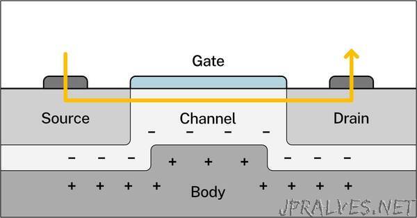
In a classic metal oxide semiconductor design (see figure), a metal electrode called the gate is placed atop a thin insulating silicon dioxide layer. Below that interface is the bulk body of the semiconductor.
On one side of the gate is an input terminal, called the source; on the other is an output (drain). Scientists investigate the dynamics of current flow by changing the “bias” voltages applied to the gate, source and drain, all of which affect how current moves.
In the new work, the NIST and Penn State researchers concentrated on one particular region that is typically only about 1 billionth of a meter thick and a millionth of a meter long: the boundary, or channel, between the thin oxide layer and the bulk semiconductor body.
“This layer is hugely important because the effect of a voltage on the metal overtop of the oxide of the transistor acts to change how many electrons are within the channel region under the oxide; this region controls the resistance of the device from source to drain,” Ashton said. “The performance of this layer is dependent on how many defects exist. The detection method we investigated was previously unable to determine how many defects were within this layer.”
One sensitive method to detect defects in the channel is called electrically detected magnetic resonance (EDMR), which is similar in principle to medical MRI. Particles such as protons and electrons have a quantum property called spin, which makes them act like tiny bar magnets with two opposite magnetic poles. In EDMR, the transistor is irradiated with microwaves at a frequency about four times higher than a microwave oven. Experimenters apply a magnetic field to the device and gradually vary its strength while measuring the output current.
At exactly the right combination of frequency and field strength, electrons at defects “flip” — reverse their poles. This causes some to lose enough energy that they recombine with holes at defects in the channel, reducing the current. The channel activity can be hard to measure, however, because the high volume of “noise” from recombination in the bulk of the semiconductor.
To focus exclusively on activity in the channel, researchers use a technique called bipolar amplification effect (BAE), which is achieved by arranging the bias voltages applied to the source, gate and drain in a particular configuration (see figure). “So because of the biasing we use in BAE and because we measure current levels at the drain,” Ashton said, “we can eliminate interference from other things going on in the transistor. We can select just defects that we care about within the channel.”
The exact mechanism by which BAE operates was not known until the team developed its model. “The only measurement results were qualitative — that is, they could tell the kinds of defects in the channel but not the number,” said co-author Patrick Lenahan, a distinguished professor of engineering science and mechanics at Penn State.
Before the model of BAE, the scheme was used strictly as a resource for applying voltages and controlling currents for EDMR measurements, which is useful for a more qualitative defect identification. The new model enables BAE as a tool to quantitatively measure the number of defects and to do so with just currents and voltages. The parameter of importance is the interface defect density, which is a number that describes how many defects are within some area of the semiconductor-oxide interface. The BAE model gives researchers a mathematical description of how the BAE current is related to the defect density.
The model, which the researchers tested in a set of proof-of-concept experiments on metal oxide semiconductor transistors, makes quantitative measurements possible. “Now we can account for the variation in charge carrier distribution throughout the channel region,” Ashton said. “This opens up the possibilities of what can be measured with a simple electrical measurement.”
“This technique can provide unique insight into the presence of these destabilizing transistor defects and a path to mechanistic understanding of their formation,” said Markus Kuhn, formerly at Intel and now senior director of semiconductor metrology and fellow at Rigaku, who was not involved in the research. “With such knowledge, there would be greater opportunity to control and reduce them in order to improve transistor performance and reliability. This would be an opportunity to further enhance design of the chip circuitry and device performance leading to better performing products.””