
“Stress and strain, applied in just the right manner, can sometimes produce amazing results.
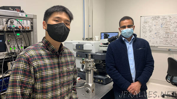
That is what researchers, led by a team at UC Berkeley’s Department of Electrical Engineering and Computer Sciences, discovered about an emerging semiconductor material — black phosphorus (BP) — used to make two types of optoelectronic devices: light emitting diodes (LEDs) and photodetectors.
Under mechanical strain, BP can be induced to emit or detect infrared (IR) light in a range of desirable wavelengths — 2.3 to 5.5 micrometers, which spans the short- to mid-wave IR — and to do so reversibly at room temperature, according to study authors Ali Javey, Lam Research Distinguished Chair in Semiconductor Processing and professor of electrical engineering, and postdoctoral fellow Hyungjin Kim. Javey is also a faculty senior scientist at the Lawrence Berkeley National Laboratory.
Their findings are significant not only for the ability to reach these wavelengths, Javey and Kim said, but to do so tunably and in one device. Current technology would require multiple bulky devices and differing semiconductor materials to achieve similar results.
They described their findings in the issue of the journal Nature published today.
Javey and Kim said that the ability to use a broader range of the IR spectrum, tunable within one device, could help meet the growing demand for applications in optical communications, thermal imaging, health monitoring, spectroscopy, chemical sensing and more. To demonstrate this flexibility, the researchers used one of their new devices to detect multiple gases.
The Berkeley-led team found that using thin layers of BP in optoelectronic devices and subjecting them to varying degrees of strain results in reversibly tunable output wavelengths over an unexpectedly large range. The output wavelength of BP and other semiconductor materials is a property known as bandgap.
The spectral range over which an optoelectronic device can operate is largely determined by the bandgap of its semiconductor material. Different approaches can be used to achieve the desired operating wavelength for a given application. For example, alloys — materials of varying composition — and strain can be used to tune the bandgap. While these approaches are indeed effective, they result in devices with fixed operating wavelengths.
“In our work, we can actively change the bandgap of the black phosphorus such that a single photodetector or LED can change its operating wavelengths within, roughly, the two- to five- micrometer range,” Kim said.
“We can go back and forth as many times as we want,” Kim said of the reversibly tunable wavelengths of BP based devices. They exploit BP’s “magical” properties, he said, specifically, its bandgap change under strain, which is much larger than those observed with conventional semiconductor materials.
“There is innovation in the device itself,” Javey said, “but the material that we are using, black phosphorus, also has inherently unique properties [bandgap and sensitivity to strain], and we’re combining those two key characteristics.”
Black phosphorus is a two-dimensional material like graphene. In a process called exfoliation, researchers use Scotch tape to lift nanometer-thin layers of the material, which is then transferred to a flexible polymer substrate, in this case polyethylene terephthalate glycol (PETG).
“Because it’s mechanically flexible, we can bend it to a desired radius and controllably apply strain to BP,” Kim said. That is, bending becomes an effective knob to modulate the BP bandgap.
Indeed, due to its puckered lattice structure, Kim said, BP shows unique strain-dependent properties which, in addition to bandgap, include tunable van der Waals interaction and piezoelectricity. Strain can be applied to BP in a reversible manner due to its thin membrane nature, he said.
In one application, the researchers used a technique called non-dispersive IR gas sensing. Because each gas has its own absorption band — that is, the amount of light it absorbs at a specific wavelength — a tunable IR LED of sufficient output wavelength range could detect, for example, carbon dioxide expelled by human breathing. That’s because the gas absorbs light at around 4.3 micrometers, within the 2.3 to 5.5 micrometer device range. Other gases detectible with tunable BP LEDs include methane and water.
An application for BP photodetectors could be thermal imaging. It could be used, for example, in night vision goggles to detect any exothermic heat source like human bodies. Such tunable photodetectors would be capable of selective thermal imaging over a range of IR wavelengths.
From the materials point of view, there is a lot of interest in identifying new semiconductors that are more efficient in this wavelength range, Javey said. “That’s when we started to look at black phosphorus because it was known already to have a bandgap that overlaps with the mid-wavelength IR. From there we looked at how we can build efficient devices like LEDs and photodetectors using this material. But what is new here is tunability — that you can actively tune the device with strain over a large wavelength range.”
Moving forward, Javey said, “I think this device concept can be applied to other parts of the spectrum, perhaps even making devices that could operate in the visible regime. That could enable new types of displays, for example, if these concepts and materials can be incorporated in a manufacturable, scalable way, with miniaturized electromechanical devices.”
Other coauthors include researchers from the University of Melbourne in Australia. Javey and Kim, as well as some other coauthors, also hold appointments in the Materials Sciences Division at Lawrence Berkeley National Laboratory.
This work was supported by the U.S. Department of Energy, the Defense Advanced Research Projects Agency and the Australian Research Council.”