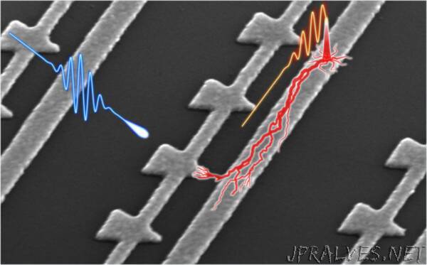
“MIT researchers develop compact on-chip device for detecting electric-field waveforms with attosecond time resolution.
Understanding how light waves oscillate in time as they interact with materials is essential to understanding light-driven energy transfer in materials, such as solar cells or plants. Due to the fantastically high speeds at which light waves oscillate, however, scientists have yet to develop a compact device with enough time resolution to directly capture them.
Now, a team led by MIT researchers has demonstrated chip-scale devices that can directly trace the weak electric field of light waves as they change in time. Their device, which incorporates a microchip that uses short laser pulses and nanoscale antennas, is easy to use, requiring no special environment for operation, minimal laser parameters, and conventional laboratory electronics.
The team’s work, published earlier this month in Nature Photonics, may enable the development of new tools for optical measurements with applications in areas such as biology, medicine, food safety, gas sensing, and drug discovery.
“The potential applications of this technology are many,” says co-author Phillip Donnie Keathley, group leader and Research Laboratory of Electronics (RLE) research scientist. “For instance, using these optical sampling devices, researchers will be able to better understand optical absorption pathways in plants and photovoltaics, or to better identify molecular signatures in complex biological systems.”
Keathley’s co-authors are lead author Mina Bionta, a senior postdoc at RLE; Felix Ritzkowsky, a graduate student at the Deutsches Elektronen-Synchrotron (DESY) and the University of Hamburg who was an MIT visiting student; and Marco Turchetti, a graduate student in RLE. The team was led by Keathley working with professors Karl Berggren in the MIT Department of Electrical Engineering and Computer Science (EECS); Franz Kärtner of DESY and University of Hamburg in Germany; and William Putnam of the University of California at Davis. Other co-authors are Yujia Yang, a former MIT postdoc now at École Polytechnique Fédérale de Lausanne (EFPL), and Dario Cattozzo Mor, a former visiting student.
The ultrafast meets the ultrasmall — time stands still at the head of a pin
Researchers have long sought methods for measuring systems as they change in time. Tracking gigahertz waves, like those used for your phone or Wi-Fi router, requires a time resolution of less than 1 nanosecond (one-billionth of a second). To track visible light waves requires an even faster time resolution — less than 1 femtosecond (one-millionth of one-billionth of a second).
The MIT and DESY research teams designed a microchip that uses short laser pulses to create extremely fast electronic flashes at the tips of nanoscale antennas. The nanoscale antennas are designed to enhance the field of the short laser pulse to the point that they are strong enough to rip electrons out of the antenna, creating an electronic flash that is quickly deposited into a collecting electrode. These electronic flashes are extremely brief, lasting only a few hundred attoseconds (a few one-hundred-billionths of one-billionth of 1 second).
Using these fast flashes, the researchers were able to take snapshots of much weaker light waves oscillating as they passed by the chip.
“This work shows, once more, how the merger of nanofabrication and ultrafast physics can lead to exciting insights and new ultrafast measurements tools,” says Professor Peter Hommelhoff, chair for laser physics at the University of Erlangen-Nuremberg, who was not connected with this work. “All this is based on the deep understanding of the underlying physics. Based on this research, we can now measure ultrafast field waveforms of very weak laser pulses.”
The ability to directly measure light waves in time will benefit both science and industry, say the researchers. As light interacts with materials, its waves are altered in time, leaving signatures of the molecules inside. This optical field sampling technique promises to capture these signatures with greater fidelity and sensitivity than prior methods while using compact and integratable technology needed for real-world applications.
This research was supported by the U.S. Air Force Office of Scientific Research through a Young Investigator Program entitled “On-Chip PHz Processing of Optical Fields using Nanostructured Electron Emitters,” and a Multi University Research Initiative (MURI) program entitled “Empty State Electronics.” The work was also supported in part by the European Research Council, the MIT-Hamburg PIER program at DESY, and SENSE.nano at MIT.”
