
“Emerging quantum technologies require a means to transmit quantum information effectively requiring new ways to reliably encode, transmit and detect quantum properties on individual particles of light, or photons.
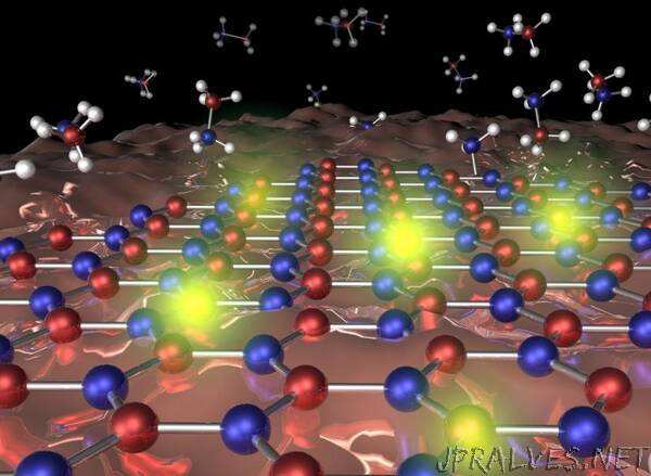
An international collaboration, led by the University of Technology Sydney, investigating the chemical structure of crystal imperfections, or defects, in the nanomaterial hexagonal boron nitride (hBN) have definitively linked the defect structure to carbon impurities introduced into the hBN lattice. The discovery enables a better understanding of the properties of these quantum light sources that could help overcome a barrier to their reliable fabrication.
Generating Quantum Light
In new research published in Nature Materials, an international multidisciplinary collaboration led by the University of Technology Sydney (UTS), has uncovered the chemical structure behind defects in white graphene (hexagonal boron nitride, hBN), a two dimensional nanomaterial that shows great promise as a platform for generating quantum light. The defects, or crystal imperfections, can act as single photon sources and an understanding of their chemical structure is critical to being able to fabricate them in a controlled way.
“hBN single photon emitters display outstanding optical properties, among the best from any solid state material system, however, to make practical use of them we need to understand the nature of the defect and we have finally started to unravel this riddle,” says UTS PhD candidate Noah Mendelson and first author of the study.
“Unfortunately, we cannot simply combine powerful techniques to visualize single atoms directly with our quantum optics measurements, so obtaining this structural information is very challenging. Instead we attacked this problem from a different angle, by controlling the incorporation of dopants, like carbon, into hBN during growth and then directly comparing the optical properties for each, “ he said.
The researchers were able to observe, for the first time, a direct link between carbon incorporation into the hBN lattice and quantum emission.
The researchers were able to observe, for the first time, a direct link between carbon incorporation into the hBN lattice and quantum emission.
Collaborative impact
By controlling the incorporation of carbon impurities during hBN growth the scientists were able to confirm that the presence and the density of incorporated single photon emitters is directly related to the level of carbon doping. While eliminating carbon completely eliminated the presence of the quantum emitters. To further confirm their hypothesis and demonstrate the deterministic fabrication of the defects, the scientists bombarded pristine hBN crystals with single carbon ions. They found again that the quantum emission centres are only created in regions bombarded by carbon, confirming that a carbon based defect gives rise to the observed quantum emission.
To complete the comprehensive study, the team, led by UTS Professor Igor Aharonovich, and chief investigator of the ARC Centre of Excellence for Transformative Meta-Optical Materials (TMOS), turned to collaborators across the world to provide the array of samples needed.
“Determining the structure of material defects is an incredibly challenging problem and requires experts from many disciplines. This is not something we could have done within our group alone. Only by recruiting collaborators from across the world whose expertise lies in different materials growth techniques could we study this issue comprehensively. Working together were we finally able to provide the clarity needed for the research community as a whole,” said Professor Aharonovich.
Novel research field emerges
The scientists also identified another intriguing feature in their study, that the defects carry spin, a fundamental quantum mechanical property, and a key element to encode and retrieve quantum information stored on single photons. The researchers also demonstrated that, unusually, the spin can be manipulated up to room temperature, typically a harsh environment for the conservation of quantum properties such as spin.
“Confirming these defects carry spin opens up exciting possibilities for future applications, as no other solid state defect has such a collection of ideal optical and spin properties at room temperature. Furthermore, the advantages of being hosted in a 2D material only bolsters the potential for integration into on-chip devices, for sensing applications, as well as for more fundamental studies such as their combination with other layered materials to create designer quantum materials” Prof. Aharonovich noted.
The work brings to the forefront a novel research field, 2D quantum spintronics, and lays the groundwork for further studies into quantum light emission from hBN. The authors anticipate their work will stimulate increased interest in the field and facilitate a range of follow up experiments such as the generation of entangled photon pairs from hBN, detailed studies of the spin properties of the system, and theoretical confirmation of the defect structure.
“This is just the beginning, and we anticipate our findings will accelerate the deployment of hBN quantum emitters for a range of emerging technologies,” concludes Mr. Mendelson.
Researchers from the Australian National University, Shanghai University, University of Nottingham, University of Würzburg, University of California and Trent University were also involved in the study
Funding
Australian Research Council, Asian Office of Aerospace Research & Development, US Department of Energy, National Computational Infrastructure (NCI), Intersect, the Shanghai University, Chinese National Natural Science Foundation, German Research Foundation, Engineering and Physical Sciences Research Council, University of Nottingham Propulsion Futures Beacon.”