
“Linking multiple copies of these devices may lay the foundation for quantum computing.
Once unimaginable, transistors consisting only of several-atom clusters or even single atoms promise to become the building blocks of a new generation of computers with unparalleled memory and processing power. But to realize the full potential of these tiny transistors — miniature electrical on-off switches — researchers must find a way to make many copies of these notoriously difficult-to-fabricate components.
Now, researchers at the National Institute of Standards and Technology (NIST) and their colleagues at the University of Maryland have developed a step-by-step recipe to produce the atomic-scale devices. Using these instructions, the NIST-led team has become only the second in the world to construct a single-atom transistor and the first to fabricate a series of single electron transistors with atom-scale control over the devices’ geometry.
The scientists demonstrated that they could precisely adjust the rate at which individual electrons flow through a physical gap or electrical barrier in their transistor — even though classical physics would forbid the electrons from doing so because they lack enough energy. That strictly quantum phenomenon, known as quantum tunneling, only becomes important when gaps are extremely tiny, such as in the miniature transistors. Precise control over quantum tunneling is key because it enables the transistors to become “entangled” or interlinked in a way only possible through quantum mechanics and opens new possibilities for creating quantum bits (qubits) that could be used in quantum computing.
To fabricate single-atom and few-atom transistors, the team relied on a known technique in which a silicon chip is covered with a layer of hydrogen atoms, which readily bind to silicon. The fine tip of a scanning tunneling microscope then removed hydrogen atoms at selected sites. The remaining hydrogen acted as a barrier so that when the team directed phosphine gas (PH3) at the silicon surface, individual PH3 molecules attached only to the locations where the hydrogen had been removed (see animation). The researchers then heated the silicon surface. The heat ejected hydrogen atoms from the PH3 and caused the phosphorus atom that was left behind to embed itself in the surface. With additional processing, bound phosphorous atoms created the foundation of a series of highly stable single- or few-atom devices that have the potential to serve as qubits.
Two of the steps in the method devised by the NIST teams — sealing the phosphorus atoms with protective layers of silicon and then making electrical contact with the embedded atoms — appear to have been essential to reliably fabricate many copies of atomically precise devices, NIST researcher Richard Silver said.
In the past, researchers have typically applied heat as all the silicon layers are grown, in order to remove defects and ensure that the silicon has the pure crystalline structure required to integrate the single-atom devices with conventional silicon-chip electrical components. But the NIST scientists found that such heating could dislodge the bound phosphorus atoms and potentially disrupt the structure of the atomic-scale devices. Instead, the team deposited the first several silicon layers at room temperature, allowing the phosphorus atoms to stay put. Only when subsequent layers were deposited did the team apply heat.
“We believe our method of applying the layers provides more stable and precise atomic-scale devices,“ said Silver. Having even a single atom out of place can alter the conductivity and other properties of electrical components that feature single or small clusters of atoms.
The team also developed a novel technique for the crucial step of making electrical contact with the buried atoms so that they can operate as part of a circuit. The NIST scientists gently heated a layer of palladium metal applied to specific regions on the silicon surface that resided directly above selected components of the silicon-embedded device. The heated palladium reacted with the silicon to form an electrically conducting alloy called palladium silicide, which naturally penetrated through the silicon and made contact with the phosphorus atoms.
In a recent edition of Advanced Functional Materials, Silver and his colleagues, who include Xiqiao Wang, Jonathan Wyrick, Michael Stewart Jr. and Curt Richter, emphasized that their contact method has a nearly 100% success rate. That’s a key achievement, noted Wyrick. “You can have the best single-atom-transistor device in the world, but if you can’t make contact with it, it’s useless,” he said.
Fabricating single-atom transistors “is a difficult and complicated process that maybe everyone has to cut their teeth on, but we’ve laid out the steps so that other teams don’t have to proceed by trial and error,” said Richter.
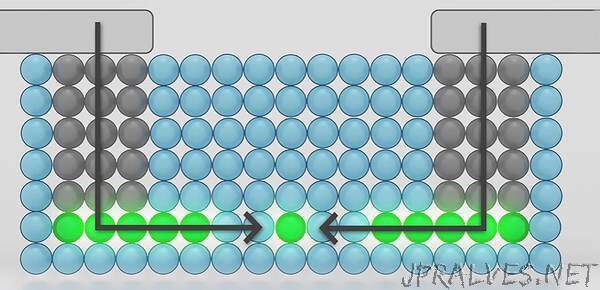
In related work published today in Communications Physics, Silver and his colleagues demonstrated that they could precisely control the rate at which individual electrons tunnel through atomically precise tunnel barriers in single-electron transistors. The NIST researchers and their colleagues fabricated a series of single-electron transistors identical in every way except for differences in the size of the tunneling gap. Measurements of current flow indicated that by increasing or decreasing the gap between transistor components by less than a nanometer (billionth of a meter), the team could precisely control the flow of a single electron through the transistor in a predictable manner.
“Because quantum tunneling is so fundamental to any quantum device, including the construction of qubits, the ability to control the flow of one electron at a time is a significant achievement,” Wyrick said. In addition, as engineers pack more and more circuitry on a tiny computer chip and the gap between components continues to shrink, understanding and controlling the effects of quantum tunneling will become even more critical, Richter said.”