
“With a plethora of semiconductor start-ups, semiconductor companies, universities, government agencies, and even device and system OEMs working on chips for artificial intelligence (AI), it’s hard to stand out from the crowd. However, a start-up called Cerebras has managed to do so. Yesterday at the Hot Chips conference held at Stanford University, Cerebras introduced a unique solution for AI deep learning that is an engineering marvel.
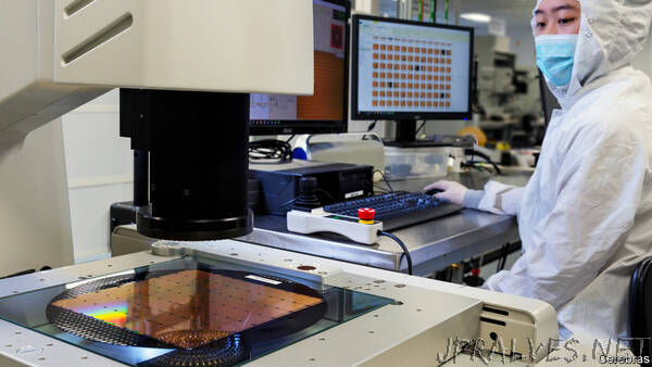
There are so many things that make the Cerebras solution unique that it is hard to know where to start. Cerebras has overcome many design, manufacturing, and packaging challenges to develop a wafer-scale solution called the Wafer Scale Engine (WSE). This means that the design uses the entire useable space of the silicon wafer as a single chip or platform. Most chips are made by placing 10’s or 100’s of instances of a chip on one wafer and then cutting up the wafer into individual chips. Using an entire wafer as a single chip has been attempted for other applications but typically abandoned over cost and yield issues. A single 300mm wafer can cost 10’s of thousands of dollars to produce. However, the smallest speck of dust or imperfection in the processing can cause the failure of a portion of a chip and often the failure of the entire chip. Manufacturing an entire wafer without an error is impossible, but Cerebras found a way around it. The Cerebras WSE is made of 84 processing tiles, similar to individual chips, and each tile has redundant processor cores, memory, and I/O. When one part of a tile fails, the extra functions are substituted in their place through software tools, making it seem like a fully functioning tile. As a result, the company can theoretically have 100% yield of all tiles on a wafer and all wafers produced.
However, the manufacturing is only one part of the equation. Another issue is the challenge of supplying power and cooling to an entire wafer-scale solution. With 400,000 programmable processor cores, 18 GB of memory, and an on-chip fabric capable of 25 petabits, the WSE comprises 1.2 trillion transistors in 46,225 mm2 of silicon real estate (for contrast, it is 56x larger than the largest GPU for AI, which is 815mm2). In addition, the WSE is rated at a whopping 15kW. If you are talking about a home battery system, solar array, or electric vehicle, a discussion of kilowatts (kW) would be normal, but for a single chip, this is over an order of magnitude more than any chip ever produced. This required innovation in the device operation, board/substrate design and cooling system, just to handle that much power and the subsequent heat.
Let’s look at each one of these innovations individually.
The first innovation is in the operation of the WSE. With such a large die array, it would be inefficient in both power and latency to send data and instructions across the chip. As a result, the software tools used in developing the neural network clump close processing tiles together into clusters and then route data through the chip in a single path. The path appears like a random maze, but it is optimized to use the entire chip and while achieving the lowest latency.
The second innovation is the substrate design to handle the power requirements. Unlike other socket-based processors, you cannot have one or even a few power connectors because just like routing data, routing power across the huge chip would be inefficient and possible damaging by creating hot spots. Power must be applied uniformly to each of the processing tiles across the wafer. Cerebras accomplished this by applying power to each tile through a special substrate rather than from routing patterns on the substrate. Think of it as having individual power pins for each processor tile.
The third innovation is the cooling. The entire 15kW chip must be cooled, and liquid cooling is the only viable option. However, if you run water or other coolant across the chip, the stream would become hot by the time it reached the opposite side of the chip, possibly damaging the chip. Cerebras overcame this challenge by having a cooling solution that has multiple zones with each zone having its own input and output water ports. So, instead of having one radiator, it has multiple radiators cooling the chip.
On top of these engineering innovations, the company develop new programmable Sparse Linear Algebra Cores (SLAC) optimized for AI processing. The SLAC skips any function that multiplies by zero, which can significantly speed the multiplication of matrices in the deep learning process while reducing power. The company also reduced the memory stack by eliminating cache and putting large amounts of high-speed memory (18 GB of SRAM) close to the processing cores. All this is connected by what the company calls the Swarm communication fabric, a 2D mesh fabric with 25 petabits of bandwidth that is designed to fit between the processor cores and tiles, including what would normally be die cut area on the wafer.
All these innovations will need to be implemented in a chassis, which is Cerebras is not discussing at this time. However, the company did indicate that more information would be available by the end of the year. Note that the Cerebras solution is designed just for AI processing. As a result, WSE will need to be connected to a host processor or processors. But the result is still a single server with what amounts to thousands of AI accelerators all packed into a single chip. While the software details are limited, the company did indicate that the WSE does support TensorFlow and other popular software frameworks.
Because of its design, the Cerebras WSE platform has advantages in latency, bandwidth, processing efficiency, and size. According to Cerebras, the WSE is 56.7 times larger than the largest GPU, has 3,000 times more on-die memory, has 10,000 times more memory bandwidth, and fits into 1/50th of the space of a traditional data center configuration with thousands of server nodes. The company has not discussed the availability of the platform or estimated cost.
Something else that separates Cerebras from the pack is that the company is focused on deep learning training. There are two forms of AI processing. One is the training of artificial neural networks, which is accomplished through of a variety of deep learning techniques and software frameworks. The other form of AI processing is inference, which is using a trained neural network to make a determination or decision. Most companies are focused on the inference processing because it will account for the vast majority of AI processing. Many of the new AI entrants claim to do both. While doing both training and inference is possible, there are tradeoffs performance and efficiency. The most efficient solutions will typically target one or the other.
Like many of the semiconductor start-ups, Cerebras has many serial entrepreneurs and industry experts that know what it takes to succeed. However, the company has chosen a completely different technical route than its peers. As Tirias Research has indicated before, we see plenty of room in AI for different platforms because no two workloads are the same. We applaud the audacious design risk that Cerebras is taking to push technologies beyond what we thought were the limits. The Cerebras solution is unique and appears to be well suited for training of very large data sets. However, cost and data center resources, especially power, will have to be taken into consideration. With the current platform, only the largest internet companies, cloud service providers, and enterprise customers are likely to be potential customers.”