
“A new optical technology may revolutionize the semiconductor industry and create brand new possibilities within sustainable electronics and data handling. The project is subsidized by Innovation Fund Denmark.
We take it for granted that a new smartphone or tablet is faster than its obsolete predecessor. It has more memory, is thinner, and its touch screen is crystal-clear with a fast response rate. In a few years it may even be flexible, allowing you to roll it up and put it in your pocket.
We expect that renewable energy from solar and wind power will become increasingly efficient and profitable, and that electric cars and trains will play a major role in a future sustainable society and for our environment.
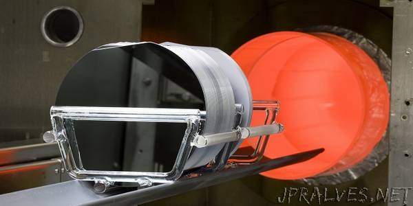
The semiconductor industry is one of the driving forces behind this development. It provides the processing power for handling the astronomical data volumes produced, and delivers efficient components for high-power electronics.
The new Innovation Fund project TRIM has a total budget of EUR 3.7 million (DKK 27 million) and is subsidized by Innovation Fund Denmark with EUR 2.6 million (DKK 19 million).
The aim is to develop optical technology based on terahertz radiation, which can measure the quality of electric and magnetic materials for the semiconductor industry. This ensures high-quality and homogeneous materials.
“Some of the key words for the continued development of a sustainable information society is increased speed, greater storage capacity and higher reliability. All of these require control and quality assurance. Terahertz technology has been the focus of research around the world for many years—now the time has come to bring a huge basic research investment into the real world and prove the value of the technology,” says Peter Uhd Jepsen, Professor, DTU Fotonik, who will be heading the project for the next three years.
The technology offers unique opportunities for completely contactless measurements—a property in high demand by industry, and an essential requirement for the characterization of e.g. 2D materials consisting of one or only a few layers of atoms.
The development of the TRIM technology takes place in close collaboration between DTU and the companies Capres A/S, Topsil GlobalWafers A/S, and NKT Photonics A/S.
The project links the world’s leading competences within terahertz and laser technology, silicon fabrication, and semiconductor materials characterization. It introduces completely new technology and methodology into a conservative and notoriously cautious industry.
“Denmark has a strong position within characterization of materials for the semiconductor industry, but there is still some way to go before we can roll out our laboratory experience to industry. The investment from Innovation Fund Denmark will help us overcome the technological and commercial barriers, which are completely natural, but must be broken down to ensure acceptance of new technologies and methods,” says Peter Uhd Jepsen.”