
“An ultracompact laser has been made using nanoscale semiconductor columns
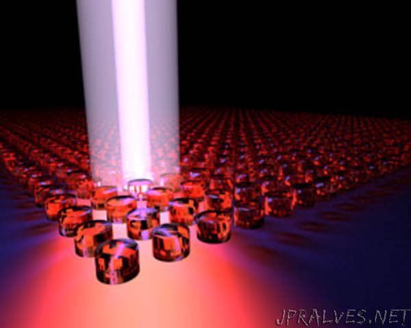
A tiny laser comprising an array of nanoscale semiconductor cylinders (see image) has been made by an all-A*STAR team1. This is the first time that lasing has been achieved in non-metallic nanostructures, and it promises to lead to miniature lasers usable in a wide range of optoelectronic devices.
Microscale lasers are widely used in devices such as CD and DVD players. Now, optical engineers are developing nanoscale lasers — so small that they cannot be seen by the human eye.
A promising method is to use arrays of tiny structures made from semiconductors with a high refractive index. Such structures act as tiny antennas, resonating at specific wavelengths. However, it has been challenging to use them to construct a cavity — the heart of a laser, where light bounces around while being amplified.
Now, Arseniy Kuznetsov, Son Tung Ha, Ramón Paniagua-Domínguez, and their colleagues at the A*STAR Institute of Materials Research and Engineering have overcome this problem by exploiting a highly unusual type of standing wave that remains in one spot despite coexisting with a continuous spectrum of radiating waves that can transport energy away. First predicted by quantum mechanics, this wave was demonstrated experimentally in optics about a decade ago.
There was an element of serendipity in the invention. “We initially planned to create a laser just based on the diffractive resonances in the array,” recalls Kuznetsov. “But after fabricating samples and testing them, we discovered this strong enhancement at a different wavelength from expected. When we went back and did further simulations and analysis, we realized that we had created these special waves.”
The demonstration is the culmination of five years of research by the team. It was a race against time, since other groups were also working on developing active nanoantennas, Kuznetsov notes. “Until now, lasing hasn’t been realized in nanoantenna structures,” he says. “So it’s a big step for the dielectric nanoantenna community.”
Their laser also has advantages over other kinds of miniature lasers. Firstly, the direction of its narrow, well-defined beam can be easily controlled — this maneuverability is often needed in device applications. Also, because the nanocylinders are quite sparsely distributed, the laser is highly transparent, which is beneficial for multilayer devices that contain other optical components.
The team is now working to develop lasers that can be excited electrically, rather than by light as in the present study, which would be a major advance toward realizing commercial nanolasers.
The A*STAR-affiliated researchers contributing to this research are from the Institute of Materials Research and Engineering and the Institute of Microelectronics.”