
“Summary
The researchers have developed a static electricity scanning system which can measure surface potential distribution at a spatial resolution of 1 mm. The system consists of a high-speed signal processing apparatus and a small-sized, high-performance array sensor which is a capacitance type.
Method created by AIST
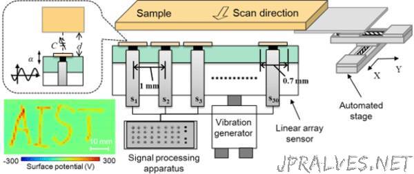
The researchers have developed a liner array sensor which comprises 30 parallel microsensors placed at intervals of 1 mm. The sensor has been miniaturized by fabricating the microsensors and the other parts using photolithography technology. They have also developed a high-speed signal processing apparatus. Using the developed array sensor that can measure weak signals and the high-speed processing apparatus, a system with high-speed scanning of an object surface at a speed of 15 mm/s and capable of visualizing distribution of surface potential at a spatial resolution of 1 mm has been developed.
Background
Smart manufacturing that automates processes using various sensors has been facilitated. However, insulating materials used in products are likely to be charged with static electricity, and ununiformly distributed static electricity on the surfaces of the materials is a factor inhibiting production. Charge distribution that is not always stationary is present inside an apparatus or products and it may cause circuit breakage due to electric discharge and quality degradation due to the attachment of minute objects such as dust. Although neutralization is performed, it is performed wholly and the effect is often unclear. Accordingly, a measuring apparatus for static electricity distribution that can scan a large area at a high speed and detecting even small defects has been demanded.
Future research plan
Upon requests, commissions, and so on from companies, the researchers begin tests to measure and evaluate static electricity distribution on various objects such as glass, printed circuit boards, films, resins, and ceramics. Also, they will develop a higher-speed and higher-spatial-resolution static electricity scanner that can measure large area, and aim to put it into practical use within a few years.”