
“Researchers: Wen Hsin Chang, AIST Researcher, the Nanoelectronics Research Institute, Toshifumi Irisawa, Senior Researcher, 3D Integration System Group of the institute, and Tatsuro Maeda, Research Manager of the institute
Summary
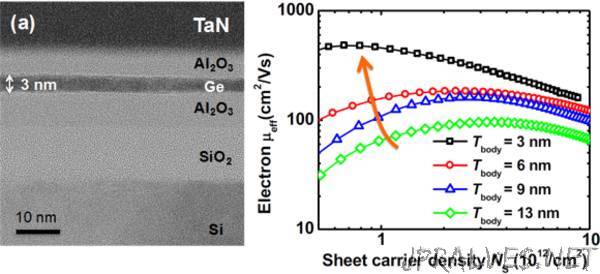
The researchers have developed a method for fabricating a uniform ultra-thin film of germanium (Ge) between two insulating layers. They have also discovered that electron mobility remarkably improved when thickness of the uniform ultra-thin Ge film was thinned below 10 nm.
New Results
The researchers have developed a semiconductor transfer technology for fabricating thin single-crystalline films of Ge with the thickness below 10 nm. Lattice matched epitaxial growth and selective etching were sophisticated and utilized. Contrary to common sense on semiconductors, electron mobility significantly increased as the thickness of the single-crystalline film of Ge was thinned. This may be attributed to modulation of Ge energy band structure.
Background
In order to reduce power consumption, research and development of Ge transistors have been pushed. As Ge transistors possess higher electron and hole mobility than that of silicon, operating voltage of Ge transistors can be decreased. However, high-performance Ge transistors still cannot be realized in mass production owing to the lack of high-quality single-crystalline thin films of Ge.
Future Plan
In order to realize high performance ultra-low power consumption Ge-LSIs, the researchers will establish a more precise thin-film forming process to improve mobility and clarify the mechanism behind the newly discovered phenomenon.”