
“A group of spintronics researchers at EPFL is using new materials to reveal more of the many capabilities of electrons. The field of spintronics seeks to tap the quantum properties of “spin,” the term often used to describe one of the fundamental properties of elementary particles – in this case, electrons. This is among the most cutting-edge areas of research in electronics today.
Researchers working in the Laboratory of Nanoscale Electronics and Structures (LANES), which is run by Professor Andras Kis, were able to quantify these quantum properties for a category of two-dimensional semiconductors called transition metal dichalcogenides, or TMDCs. Their research projects, which were published recently in ACS Nano and today in Nature Communications, confirm that materials like graphene (C), molybdenite (MoS2) and tungsten diselenide (WSe2) offer, either alone or by combining some of their characteristics, new perspectives for the field of electronics – perspectives that could ultimately lead to smaller chips that generate less heat.
“With the methods we’ve recently developed, we’ve shown that it is possible to access the spin in these TMDC materials, quantify it and use it to introduce new functionalities,” says Kis.
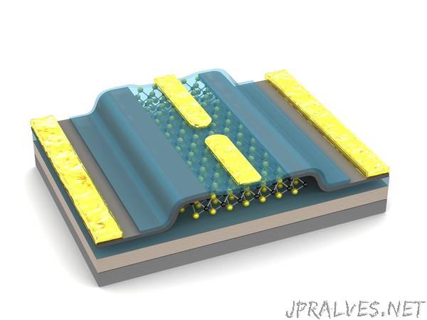
The device developed at the LANES is composed of monolayer MoS2 is the active channel, encapsulated between atomically flat h-BN layers and contacted to multilayer graphene.
This all takes place at an extremely small scale. In order to access these quantum properties, the researchers must work with high quality materials. “If we want to examine certain characteristics of electrons, including their energy, we need to be able to watch them move over relatively long distances without there being too much dispersion or disruption,” explains Kis.
In the form of waves
The researchers’ method allows them to obtain samples of sufficient quality both to observe how electrons move around in the form of waves and to quantify their energy.
But the LANES team was also able to access another quantum property. Spins of electrons and holes in this type of a 2D semiconductor can be in one of two states, which are conventionally described as being oriented upward – spin up – or downward – spin down. Their energy will be slightly different in each of these two states. That’s called spin splitting, and the EPFL researchers have measured it for the first time for electrons in TMDC materials.
In the second publication, the researchers wrote about how they used the spin splitting in a TMDC in order to introduce polarized spin currents in graphene without using a magnetic field.
These discoveries are a step forward for the emerging field of spintronics and make it increasingly likely that a different property of charge carriers – i.e. spin, in addition to the electrical charge – will play a role in tomorrow’s electronic devices.
The work was performed in collaboration with Takashi Taniguchi and Kenji Watanabe from NIMS Japan (ACS Nano and Nature Comm. papers) and Barbaros Özyilmaz from National University of Singapore (ACS Nano paper).”