
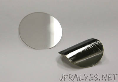
“What would a simple technique to remove thin layers from otherwise thick, rigid semiconductor crystals mean for the semiconductor industry? This concept has been actively explored for years, as integrated circuits made on thin layers hold promise for developments including improved thermal characteristics, lightweight stackability and a high degree of flexibility compared to conventionally thick substrates. In a significant advance, a research group from IBM successfully applied their new “controlled spalling” layer transfer technique to gallium nitride (GaN) crystals, a prevalent semiconductor material, and created a pathway for producing many layers from a single substrate. As they report in the Journal of Applied Physics, from AIP Publishing, controlled spalling can be used to produce thin layers from thick GaN crystals without causing crystalline damage. The technique also makes it possible to measure basic physical properties of the material system, like strain-induced optical effects and fracture toughness, which are otherwise difficult to measure. Single-crystal GaN wafers are extremely expensive, where just one 2-inch wafer can cost thousands of dollars, so having more layers means getting more value out of each wafer. Thinner layers also provide performance advantages for power electronics, since it offers lower electrical resistance and heat is easier to remove.”