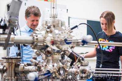
“Imagine patterning and visualizing silicon at the atomic level, something which, if done successfully, will revolutionize the quantum and classical computing industry. A team of University of Alberta scientists has done just that, led by a world-renowned physicist and his up-and-coming protégé. PhD student Taleana Huff teamed up with her supervisor Robert Wolkow to channel a technique called atomic force microscopy—or AFM—to pattern and image electronic circuits at the atomic level. This is the first time the powerful technique has been applied to atom-scale fabrication and imaging of a silicon surface, notoriously difficult because the act of applying the technique risks damaging the silicon. However, the reward is worth the risk, because this level of control could stimulate the revolution of the technology industry.”
