Content for AD75019

AD75019

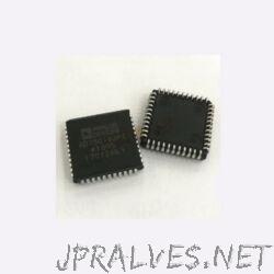
The AD75019 contains 256 analog switches in a 16 × 16 array. Any of the X or Y pins may serve as an input or output. Any or all of the X terminals may be programmed to connect to any or all of the Y terminals. The switches can accommodate signals with amplitudes up to the supply rails and have a typical on-resistance of 150 Ω. Data is loaded serially via the SIN input and clocked into an on-board 256-bit shift register via SCLK. When all the switch settings have been programmed, data is transferred into a set of 256 latches via PCLK. The serial shift register is dynamic, so there is a minimum clock rate of 20 kHz. The maximum clock rate of 5 MHz allows loading times as short as 52 μs. The switch control latches are static and will hold their data as long as power is applied.

VirtualComponent

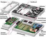
“Prototyping electronic circuits is an increasingly popular activity, supported by researchers, who develop toolkits to improve the design, debugging, and fabrication of electronics. Although past work mainly dealt with circuit topology, in this paper we propose a system for determining …