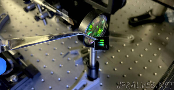
“ICFO researchers report in Nature Photonics on having achieved a solution-processed infrared laser at room temperature compatible with CMOS technology and tunable to emit in the telecommunications window.
Lasers, devices that emit light in one direction, with photons traveling at one specific frequency and all with the same phase (coherent), govern the way we communicate today. Although lasers are known to most people as little torches emitting high purity color beams, the workhorse of lasers is actually in the infrared part of spectrum, where our eyes cannot see. The reason for this is that optical fibers are highly transparent to the infrared (1.3-1.6 um), allowing efficient optical transmission with very high data rates. Moreover, infrared lasers have minimum overlap with ambient light and are considered eye-safe, allowing their use in LIDAR (light detection and ranging) applications for 3D imaging, automotive and free-space communications. To date, infrared lasers are mainly made with Erbium-doped fibers or III-V epitaxial semiconductors1, imposing certain limitations in their manufacturing and their easy integration with electronics.
An important feature to take into account while working with lasers is the optical gain. The optical gain describes how well the light can be amplified in the system. If one could find a new optical gain material platform that can be produced with low cost in high volumes and can be integrated on a variety of substrates and form factors, this would definitely unleash a whole new realm of applications. Imagine such material that can be conformally coated along optical fibers or directly deposited atop CMOS silicon. Even better, imagine it to possess facile bandgap tunability so that the emission wavelength of the laser can be readily tuned across the infrared. Such solution could lead to inter- or intra-chip optical communications offering lower power consumption, low cost and higher data rates or enable multi-spectral 3D imaging capabilities.
Colloidal quantum dot (CQD) technology is based on a solution processed optoelectronic material platform that has demonstrated already its potential for infrared optoelectronics with high performance CMOS compatible photodetectors and light emitting diodes (LEDs). The realization of an infrared CQD laser though had remained elusive.
Now, in a recent paper published in Nature Photonics, ICFO researchers Guy Whitworth, Mariona Dalmases, and Nima Taghipour, led by ICREA Prof. at ICFO Gerasimos Konstantatos have reported the achievement of a colloidal quantum-dot-based infrared laser source operating at room temperature, compatible with CMOS technology and tunable to emit in the telecommunications window, an important milestone needed for classical or quantum communications.
Previous to this finding, the team had already been working on an experiment where they were able to demonstrate stimulated emission and optical gain of quantum dots on thin films, but what they were lacking was actually inserting this setup into a cavity to achieve lasing.
Infrared QD Lasing at room temperature
To find the ideal cavity for the experiment, the team of researchers took a distributed feedback cavity (DFB), spincoating atop a thin layer of PbS CQDs as the optical gain medium. By concomitantly tuning the size of the dots and the geometrical characteristics of the DFB to optimize the cavity resonance with the gain spectrum of the quantum dots they managed to demonstrate lasing emission across the eye-safe optical communication infrared spectrum and at room temperature, thus, possibly finding the last piece of the jigsaw puzzle for silicon photonics.
In addition, the researchers went a little further and engineered the surface of the dots in order to suppress electronic trap states in order to favor stimulated emission. They made use of a robust doping of the quantum dots to demonstrate lasing emission at lower pumping intensities, an achievement that opens a new path towards more practical implementations.
As Prof. Gerasimos Konstantatos comments, “the results of this study are considered a major breakthrough in the field of CQD optoelectronics. This discovery may facilitate fully integrated silicon photonics, paving the way towards low-cost solution processed and CMOS integrated lasing sources for on-chip comm or LIDAR applications. Before, further advances are needed to optimize the material in order to demonstrate lasing under continuous wave or nanosecond excitation, which makes our next milestone.””
