“In recent years, engineers worldwide have been trying to create electronic components that are increasingly flexible and versatile, as this could enable the fabrication of more sophisticated devices and robotic systems, such as electronic skins (e-skins) or wearable sensors. The overall objective of this particular area of research is to develop flexible electronics that can be manufactured and implemented on a large scale, but that also exhibit a high device density and excellent performance.
A class of materials with particular promise for developing flexible electronic parts are two-dimensional (2-D) semiconductors, such as molybdenum disulfide (MoS2). While this material has many advantageous mechanical, optical and electronic properties, it has so far proved challenging to build large-scale, flexible integrated circuits with a high device density and high performance using MoS2.
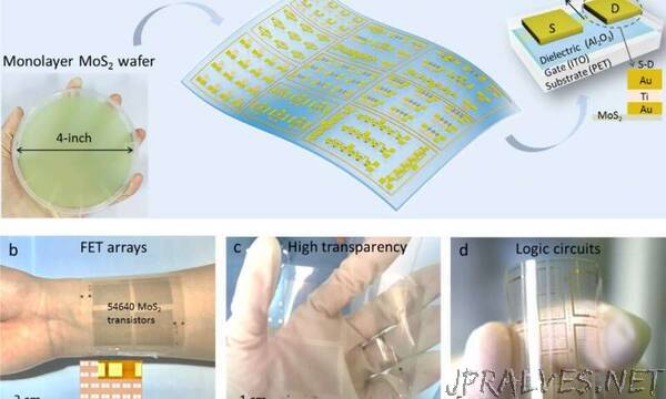
Researchers at the Chinese Academy of Sciences have recently fabricated a new flexible and transparent MoS2-based transistor that could be manufactured on a large scale. This transistor, presented in a paper published in Nature Electronics, was created using a variant of the conventional vapor deposition process.
“Two-dimensional (2-D) materials such as molybdenum disulfide (MoS2) have the potential to be the new building blocks for flexible electronics owning to their naturally thinness and flexibility,” Guangyu Zhang, one of the researchers who carried out the study, told TechXplore. “However, fabrication of large scale flexible electronic devices with high performance is still very challenging. In this work, we tried to develop prototypes of large scale flexible and transparent electronics, based on our recent progress in the wafer-scale epitaxy of high quality monolayer MoS2.”
The transistor designed by Zhang and his colleagues was fabricated by transfer of wafer-scale monolayer MoS2 on a flexible substrate. These layers can be fabricated using standard micro-fabrication technologies, which means that they could easily be produced in large quantities.
The researchers used an adapted version of atomic layer deposition (ALD), a technique typically used to coat surfaces with thin films. The alternative ALD method they employed improved the uniformity of their transistor’s high-k dielectric layer (Al2O3). In addition, they used Au/Ti/Au as source/drain contact electrodes, achieving good electrical contact.
The transistor has a high device density and a yield of 97%, as well as high on/off ratios (1010), current densities (~35 μA μm−1), mobilities (~55 cm2 V−1 s−1) and flexibility. Moreover, using the same fabrication process, the researchers were able to fabricate a variety of flexible integrated logic circuits, including inverters, NOR gates, NAND gates, AND gates, random access memory and five-stage ring oscillators.
“The large-scale flexible transistors we fabricated exhibit high device densities, yield and performances,” Zhang said. “More importantly, the device density is about 1500 transistors per cm2, it’s much higher than those achieved in previous works.”
The recent paper authored by this team of researchers introduces a promising method for fabricating large-scale MoS2-based flexible devices. In the future, this method could enable the development of flexible electronic devices that are thinner, smaller and better performing.
“In our next studies, we will continue optimizing the growth process to improve the quality of MoS2 films,” Zhang said. “In addition, we plan to further improve the device performance, increase the integration level of flexible devices and investigate more promising applications for our transistors, such as flexible memory and synaptic devices, sensors, photodetectors and so on.”“
