
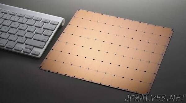
“A few years ago, we started to see researchers discussing an old manufacturing idea first explored in the 1980s: Wafer-scale processing. The idea of WSP is straightforward: Instead of dicing a wafer into individual chips and then packaging those chips for resale, build a single core or collection of cores using much, if not all, of the wafer for a single chip.
The AI/machine learning startup Cerebras has revived the idea of wafer-scale processing for a first-generation processor we covered last year. The “old” Cerebras Wafer Scale Engine (CWSE) was a 16nm wafer with 400,000 AI cores, 1.2T transistors, 18GB of onboard memory, 9 PB/s of total memory bandwidth, and 100Pb/s of total fabric bandwidth. The new version of the CWSE is supposedly even larger:
850,000 AI-optimized cores
2.6 Trillion Transistors
TSMC 7nm Process
That’s a whole lot of transistors. And cores. And probably power consumption, though the data from other companies suggests that the shift from 16nmFF to 7nm offers some significant power savings. Cerebras’ next-generation wafer-scale engine will present additional details today at Hot Chips, but so far it’s been one of the breakout darlings of the AI market.
Cerebras leverages a macroscopic approach to a microscopic problem. Ironically, chiplets and wafer-scale designs are both attempts to find a solution to the packaging and power efficiency problems of modern computing. Chiplets focus on optimizing die area and breaking a processor up into functional blocks that make the most sense for the process nodes they are deployed into. Chiplets refute the longstanding Moore’s law tenet that integration is always best and focus on integrating the components where the approach still makes sense. Wafer-scale processing also deals with integration — but from the perspective of the system as a total platform, it bypasses a lot of integration as well in favor of a fundamentally different relationship between functional blocks.
Traditionally, a CPU or GPU is a much smaller piece of silicon (limited by the maximum reticle size of the foundry, if nothing else) bonded to a package, mounted on a PCB. A single motherboard mounting 4-10 accelerator boards is an integrated system as well, and one with a lot of inefficiencies inside of it, once you start considering wire delay and overall power consumption. By stitching cores together, Cerebras bypasses the manufacturing limits that would normally prevent a wafer-scale processor from being feasible in the first place. A different approach to integration, in both cases, yields fundamental improvements where the same old way of doing things has begun to fail us.
Of course, there is one major difference between chiplets and WSE: Chiplets are already available in AMD’s consumer products, whereas wafer-scale engines draw ~15kW of power and are only available for personal installation into your evil lair and/or moon base.”