
“Researchers at C2N, in co-operation with CEA LETI and STMicroelectronics, have demonstrated a power-efficient and high-speed silicon-germanium avalanche photo-receiver. The device is fully compatible with accessible semiconductor technology and fiber-optic links operated at telecom waveband standard.
Owing to its low-cost, high-yield, and dense integration ability, silicon nanophotonics is a good candidate to tackle the needs of exponentially growing communications in data centers, high-performance computers, and cloud services. To this end, a great number of nanophotonic functions are now available on a single chip, as they take advantages of silicon-foundry process maturity. Among these different functions, optical photodetectors have been at the forefront of research interest since the early days of integrated nanophotonics. To date, most photodetectors make use of crystalline semiconductors from III-V and group-IV material classes to build optical receivers as those materials are broadly harnessed by microelectronic industry. III-V compounds (i.e. Indium Gallium Arsenide (InGaAs) and Indium Gallium Arsenide Phosphide (InGaAsP)) provide the most mature direct bandgap material system with well-mastered photodetector designs and fabrication flows. However, III-V detectors suffer from severe challenges such as overly high voltage supplies, costly manufacturing outside CMOS (complementary metal-oxide-semiconductor) foundries or complex hybrid / heterogeneous integration with other photonic platforms. In contrast, photodetectors made out of silicon and germanium (group-IV materials) are presently a mature alternative leveraging on low-cost and versatile production with a foundry-compliant monolithic integration on a single chip.
Silicon-germanium-based semiconductor avalanche photodiodes that transform signals from an optical to an electrical domain for low optical power are highly more sensitive than common Metal-semiconductor-metal and PIN diodes. Avalanche photodiodes are the most appealing for advanced power-efficient and high-speed applications as they capitalize on an internal multiplication gain, which enables generation of multiple photo-carriers per one absorbed photon, and thus intrinsically boosting the device performance. Nevertheless, silicon-germanium avalanche photodetectors have their own shadows and shortcomings. Strong electric fields are required to initiate carrier’s multiplication, which also emits excess noise. Avalanche devices are also challenged by operation under higher voltage supplies and/or they detect only low-to-moderate bit rates.
In a work published in the Optica journal, researchers at C2N, in collaboration with CEA LETI and STMicroelectronics, have succeeded in achieving a trustworthy 40 Gbps on-chip signal detection at mainstream telecommunication wavelengths. This was possible thanks to the realization of cost-effective and CMOS-compatible avalanche photodiodes with hetero-structured silicon-germanium junction.
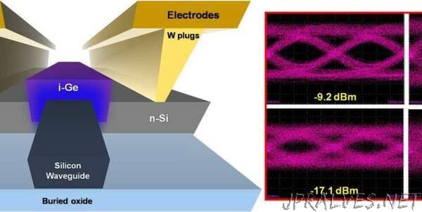
The silicon-germanium avalanche photodetectors were processed in CEA LETI’s cleanroom facilities using an open-access photonic platform for monolithic integration and conventional CMOS tools. To fully quantify the opto-electrical performance, fabricated devices were characterized at the C2N thanks to the lab skills in optical high-frequency experiments. The avalanche photodetectors essentially are simple hetero-structured PIN diodes driven with sub-10V bias voltage. The key enabler towards superior opto-electrical performance is the compact p-i-n diode with sub-µm junction area. The PIN diode benefits from strongly localized impact ionization process taking place at hetero-structured silicon-germanium interfaces. The shrinked electrical structure of the photodiode leverages exceptional low-noise properties of silicon and the localized avalanche multiplication helps suppressing parasitic excess-noise thanks to a dead space effect. In turn, this enables realization of an advanced on-chip photonic receiver with simultaneous high-speed, low-noise and energy-friendly operation at market-appealing telecommunication wavelengths. As a result, credible power sensitivities of -13 dBm and -11 dBm were measured for transmission bit rates 32 Gbps and 40 Gbps, respectively.
These results open up bountiful opportunities for chip-scale nanophotonics in modern optoelectronic and communication areas that fuse many facets of daily life. Thus, demonstrated photo-receivers are envisioned to take place in data transmission systems at an attractive telecom waveband, including surging areas of data centers, cloud and high-computing servers, or chip-scale interconnects, to name but a few.”