
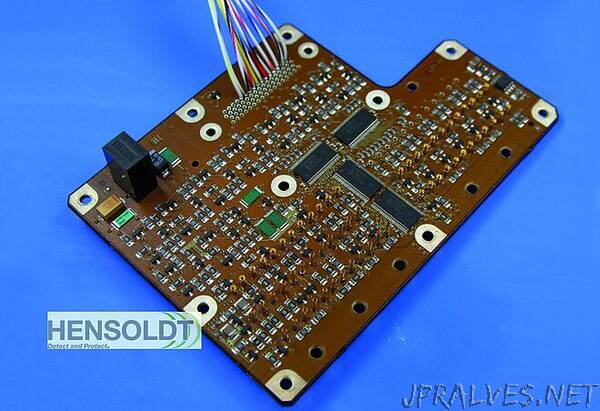
“Sensor solutions provider HENSOLDT together with the leading Additively Manufactured Electronics (AME)/Printed Electronics (PE) provider, Nano Dimension, has achieved a major breakthrough on its way to utilizing 3D printing in the development process of high-performance electronics components. Utilizing a newly developed dielectric polymer ink and conductive ink from Nano Dimension, HENSOLDT succeeded in assembling the world-wide first 10-layer printed circuit board (PCB) which carries high-performance electronic structures soldered to both outer sides. Until now, 3D printed boards could not bear the soldering process necessary for two sided population of components.
“Military sensor solutions require performance and reliability levels far above those of commercial components.” says HENSOLDT CEO, Thomas Müller. “To have high-density components quickly available with reduced effort by means of 3D printing gives us a competitive edge in the development process of such high-end electronic systems.”
“Nano Dimension’s relationship with HENSOLDT is the type of partnership with customers we are striving for,” commented Yoav Stern, Nano Dimension President & CEO. “Working together and learning from HENSOLDT led us to reach a first-of-its-kind in-depth knowledge of polymer materials applications. Additionally, it guided us in the development of Hi-PEDs (High Performance Electronic Device) that create competitive edges by enabling unique implementations with shortest time to market.””