
“Electronics should get smaller, faster, and above all more energy-efficient. These themes are also present in several research groups at the Paul Scherrer Institute PSI. From incremental improvements to complete rethinking – who is currently working on what?
Yasin Ekinci holds a slice of silicon in his hand. The interim head of the PSI Laboratory for Micro and Nanotechnology describes how computer chips are made from such discs. For around sixty years, manufacturers have used photolithography to do this. Ekinci translates: That means writing on stone with light. The stone is a silicon wafer like this one here, and the writing is done with ultraviolet light. To fabricate chips with ever-denser circuitry and more transistors, the writing had to be ever-smaller. This in turn is only possible by changing to light with still shorter wavelengths.
The standard for fifteen years has been ultraviolet light with a wavelength of 193 nanometres – one nanometre is one-millionth of a millimetre. Now chip manufacturing is facing a switch to extreme ultraviolet (EUV) light with a wavelength of only 13.5 nanometres. For that, completely new technology is needed, and we are contributing to its development, Ekinci says. For better understanding, the expert adds: During chip fabrication, the silicon is coated with photoresist. The conductor paths and transistors are projected onto it with UV light. This light-sensitive layer is then developed like an old-fashioned photograph.
Yasin Ekinci: A new photoresist for smaller structures
To produce still smaller structures with extreme ultraviolet light, a new photoresist is needed: The companies that are developing these come to us at PSI to test their potential products: With EUV light from the Swiss Light Source SLS, they write on their new photoresist, Ekinci explains, proudly adding: The smallest structure fabricated to date with photolithography was made at PSI. The world record from Ekinci’s team: a regular pattern made from parallel lines just seven nanometres wide, produced with EUV light at SLS. That corresponds to an arrangement of components sixteen times more dense than in today’s computer chips. The first chips produced with EUV light are expected to come on the market in 2019 or 2020. EUV lithography should help maintain what’s called Moore’s Law: a computer industry rule of thumb from the 1960s according to which, up to the present, key figures such as storage density and computing power double every one to two years. But experts are convinced that, in the long run, making everything smaller and smaller will not be enough.
Hans Sigg: Lasers on the chip
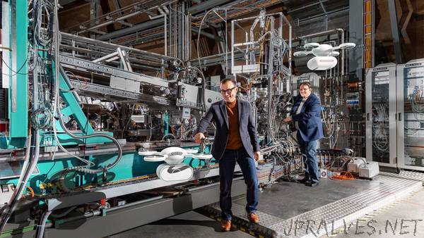
Original approaches are called for, says Rolf Allenspach, manager at the IBM research laboratory in Rüschlikon, Switzerland. In addition, for chips in mobile phones and laptops, the top priority is no longer performance, but rather energy-efficiency. This is a paradigm shift that has changed chip development, says the IBM researcher, who frequently collaborates with PSI researchers. Allenspach stresses: PSI is needed. Switzerland as a research location benefits greatly from the local large-scale research facilities and from the high-tech culture that attracts exceptionally well educated people.
PSI is needed. Switzerland as a research location benefits greatly from the local large-scale research facilities and from the high-tech culture.
Rolf Allenspach, manager at the IBM research laboratory in Rüschlikon
One idea on how to speed up communication within a chip is being pursued by Hans Sigg, head of the PSI research group on quantum technologies: We want to install tiny lasers on the chip. This could make the electronics work much more efficiently, because light too can transmit data. It is fast, and the beams can intersect, enabling a new, denser layout of elements on the chip. In optical fibre networks today, light signals are transported over long distances with practically no loss, but integrating light into the chip has not yet been successful. We are trying, among other things, to do it with germanium under tensile stress, Sigg explains. If you pull germanium apart, you can make it emit light. So far, however, this only works at low temperatures. We still don’t know if we will succeed, Sigg says. But that’s in the nature of research.
Thorsten Schmitt: How electrons flow
Thorsten Schmitt sees it in a similar way: It’s only when we work on fundamental questions that new discoveries can occur, says the head of the PSI research group for spectroscopy of novel materials. He is standing in the circular building of SLS in an experiment area where the X-ray beam terminates at two stations – in a complex, five-metre-long instrument as well as a large hemisphere. With this setup the researchers have been able to show how a component made from gallium nitride, which is already used in smartphones, can be further improved. Here researchers can look inside materials and watch the electrons flow, thus carrying out experiments on the living transistor. Schmitt’s special focus is on exotic materials that can be switched between insulating and electrically conductive behaviour. They consist of certain metal atoms and oxygen. Such so-called transition metal oxides are good candidates for particularly reliable transistors, Schmitt says.
Ekaterina Pomjakushina: Massless through new materials
For their investigations, the researchers need material samples of the highest quality. Ekaterina Pomjakushina and her team grow perfect crystals. The head of the PSI research group for solid-state chemistry opens the door to her lab: Here’s our monster, she says with a laugh, pointing to the big, snow-white special oven. Its interior is lined with brightly polished mirrors. The oven works optically, Pomjakushina explains. The light of a xenon lamp is focused by the mirrors so that the temperature reaches 3000 degrees. Here crystals grow from different starting materials, assembled beforehand in smaller ovens. Doing this requires a lot of intuition in addition to chemical knowledge. It’s like in the kitchen, the scientist says: If you want to prepare a complicated soup, you have to put the ingredients into the pot in the right order and, in the end, add the right spices. Then you get something wonderful.
What the researchers find inspiring is something that looks unimpressive: a thin, dull, black rod a few centimetres long. Pomjakushina explains: This is what most of the crystals we grow for their interesting electronic or magnetic properties look like. That also includes the material that Pomjakushina’s co-worker Pascal Puphal is studying: a so-called Weyl semimetal. In it, the electrons behave as if they had no mass – that is, like light, Puphal explains. That would be ideal for fast transistors. But the physicist knows: We are still a long way from an application. Now, to gain better understanding of the physical processes, further studies at PSI’s neutron source SINQ are planned.
Jonathan White: Skyrmions as bits of the future
In nature, neutrons occur in atomic nuclei. At SINQ they are knocked out of lead, decelerated, and guided to samples. If you want to study magnetism, neutrons are superbly suited, says Christof Niedermayer, group leader in the laboratory for neutron scattering and imaging. Magnetic hard drives will also be needed in the future, above all for the storage of large amounts of data. On these the information is stored as a series of small areas whose magnetisation points in one or the opposite direction – a series of zeroes and ones.
Perhaps tiny magnetic vortices called skyrmions will one day take on the role of these memory bits. PSI researcher Jonathan White is intensively occupied with these little vortices, and he tells about a recent conference where industry also showed interest in the topic. White is currently searching for a material in which skyrmions significantly smaller than before can be realised even at room temperature.
Marisa Medarde: Storage thanks to coupled properties
Another current magic word is multiferroics. Marisa Medarde, head of the PSI research group for physical properties of materials, investigates these special compounds whose magnetic and electrical properties are coupled together. On multiferroics, magnetic data could easily be stored by means of electrical voltage. That would be faster and more energy-efficient than the magnetic write heads in use today.
Frithjof Nolting: Switching bits with laser light
Alternatively, also for this purpose you could use laser light. We have found out that you can also switch the magnetic bits with a laser pulse, says Frithjof Nolting, head of the laboratory for condensed matter at PSI. Here too the advantage would be faster storage with lower energy consumption. At the moment Nolting and his research group are trying to confirm or disprove theoretical predictions. When I began to get interested in magnetism, I really just wanted to do fundamental research and understand what’s happening on this small magnetic scale, says the nanoscientist: However, our research could now contribute to further improvements in hard drives. “