
“Scientists from Nanyang Technological University, Singapore (NTU Singapore), in collaboration with researchers from the Massachusetts Institute of Technology (MIT) in the United States and the Skolkovo Institute of Science and Technology in Russia, have developed a machine learning approach that can predict changes to the properties of materials from straining the material.
This work could lead to the possibility of engineering new materials with tailored properties for potential use in communications, information processing, and energy fields.
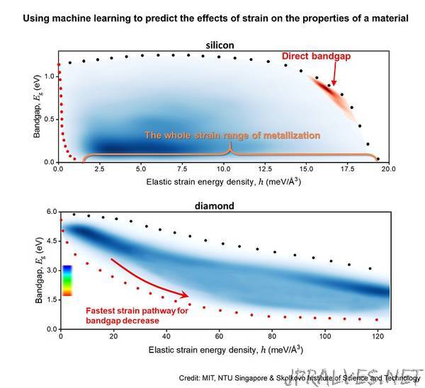
In a paper published today (12 Feb) in the Proceedings of the National Academy of Sciences, the authors demonstrated their use of Artificial Intelligence to identify the most energy-efficient strain pathways that could transform diamond into more effective semiconductors.
When a semiconductor material is bent or strained, the atoms in its structure are perturbed, thus changing its properties such as how it conducts electricity, heat or the transmission of light. This process is known as ‘strain engineering’.
Conventional methods of studying and mapping the effects of strain engineering on a material rely on trial and error lab experiments and computer modelling on a limited scale.
As a prelude to this work, last year the NTU Singapore and MIT authors reported in Science , that diamond nanoneedles could be bent and stretched as much as 9 per cent, which was surprising given that diamond is the hardest natural material known.
And in earlier research with industrial applications, “strain engineering” was used on silicon processor chips, where a one per cent strain allowed electrons to move faster, resulting in up to 50 per cent higher processing speeds.
Professor Subra Suresh, President of NTU Singapore and a senior author of the study said their new method used machine learning to predict the effects of strain on the properties of a material. This makes it possible to calculate the almost infinite possible combinations of material strain in a six-dimensional strain space.
“Now we have this reasonably accurate method that drastically reduces the complexity of the calculations needed,” said Prof Suresh, who is a former Dean of Engineering at MIT.
“Our research is an illustration of how recent advances in seemingly distant fields such as material physics, artificial intelligence, computing, and machine learning can be brought together to advance scientific knowledge that has strong implications for industry application.”
Customising material properties through strain
While conventional ways of altering semiconductors such as chemical doping – adding a new element to a material – could affect and change its properties permanently, the nonlinear elastic strain considered here is reversible, which means it can be applied and removed depending on need, explained Professor Ju Li, Battelle Energy Alliance Professor of Nuclear Science and Engineering and Materials Science and Engineering at MIT.
However, identifying and applying the full potential of strain-engineered materials is very difficult, due to the daunting range of possibilities. Strain can be applied in any of six different and independent ways (in three different dimensions, each one of which can produce strain in-and-out or sideways), and with nearly infinite gradations of degree, so the total number of possibilities are impractical to explore simply by trial and error.
“It quickly grows to 100 million calculations if we want to map out the entire elastic strain space,” says Prof Li, who is also a Professor of Materials Science and Engineering.
In this study, the team examined the effects of strain on the bandgap, a key electronic property of semiconductors, in both silicon and diamond.
Using their neural network algorithm, they predicted with high accuracy how different amounts and orientations of strain would affect the bandgap.
Being able to tune the bandgap could improve the efficiency of semiconductor materials such as a silicon solar cell, increasing the energy harnessed from light while making it a thousand times thinner, thus reducing the cost needed for materials, transportation and infrastructure.
Diamond has shown great potential as a semiconductor material with superior intrinsic properties, which are ideal for high-frequency devices like radios in satellite communications, and power electronics used for mobile networks and electrical power grids.
The work was undertaken by a multidisciplinary research team comprising Prof Subra Suresh from NTU; MIT Prof Ju Li, MIT principal research scientist and NTU Visiting Professor Dr Ming Dao, and graduate student Zhe Shi from MIT; as well as Evgeni Tsymbalov and Alexander Shapeev from the Skolkovo Institute of Science and Technology.
In addition to the bandgap, their method can also be used to study and predict other properties of materials, such as electronic, photonic and magnetic behaviours.
The work points to potential new opportunities to create materials for electronic, optoelectronic, and photonic devices that could find uses for communications, information processing, and energy applications.”