
“A KAIST research team developed a silicon optical phased array (OPA) chip, which can be a core component for three-dimensional image sensors. This research was co-led by PhD candidate Seong-Hwan Kim and Dr. Jong-Bum You from the National Nanofab Center (NNFC).
A 3D image sensor adds distance information to a two-dimensional image, such as a photo, to recognize it as a 3D image. It plays a vital role in various electronics including autonomous vehicles, drones, robots, and facial recognition systems, which require accurate measurement of the distance from objects.
Many automobile and drone companies are focusing on developing 3D image sensor systems, based on mechanical light detection and ranging (LiDAR) systems. However, it can only get as small as the size of a fist and has a high possibility of malfunctioning because it employs a mechanical method for laser beam-steering.
OPAs have gained a great attention as a key component to implement solid-state LiDAR because it can control the light direction electronically without moving parts. Silicon-based OPAs are small, durable, and can be mass-produced through conventional Si-CMOS processes.
However, in the development of OPAs, a big issue has been raised about how to achieve wide beam-steering in transversal and longitudinal directions. In the transversal direction, a wide beam-steering has been implemented, relatively easily, through a thermo-optic or electro-optic control of the phase shifters integrated with a 1D array. But the longitudinal beam-steering has been remaining as a technical challenge since only a narrow steering was possible with the same 1D array by changing the wavelengths of light, which is hard to implement in semiconductor processes.
If a light wavelength is changed, characteristics of element devices consisting the OPA can vary, which makes it difficult to control the light direction with reliability as well as to integrate a wavelength-tunable laser on a silicon-based chip. Therefore, it is essential to devise a new structure that can easily adjust the radiated light in both transversal and longitudinal directions.
By integrating tunable radiator, instead of tunable laser in a conventional OPA, Professor Hyo-Hoon Park from the School of Electrical Engineering and his team developed an ultra-small, low-power OPA chip that facilitates a wide 2D beam-steering with a monochromatic light source.
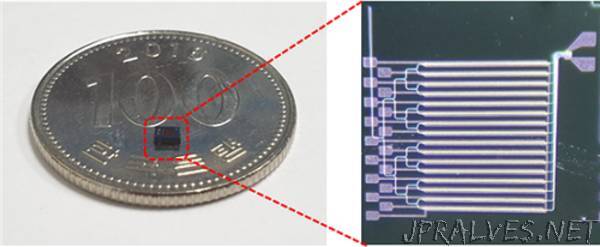
This OPA structure allows the minimizing of the 3D image sensors, as small as a dragonfly’s eye.
According to the team, the OPA can function as a 3D image sensor and also as a wireless transmitter sending the image data to a desired direction, enabling high-quality image data to be freely communicated between electronic devices.
Kim said, “It’s not an easy task to integrate a tunable light source in the OPA structures of previous works. We hope our research proposing a tunable radiator makes a big step towards commercializing OPAs.”
Dr. You added, “We will be able to support application researches of 3D image sensors, especially for facial recognition with smartphones and augmented reality services. We will try to prepare a processing platform in NNFC that provides core technologies of the 3D image sensor fabrication.”
This research was published in Optics Letters on January 15.”