
“Boron nitride is a semiconductor that could be used to make electrical equipment able to convert power more efficiently than silicon wafer technologies, up to three to 4% more efficiently than what is possible today.
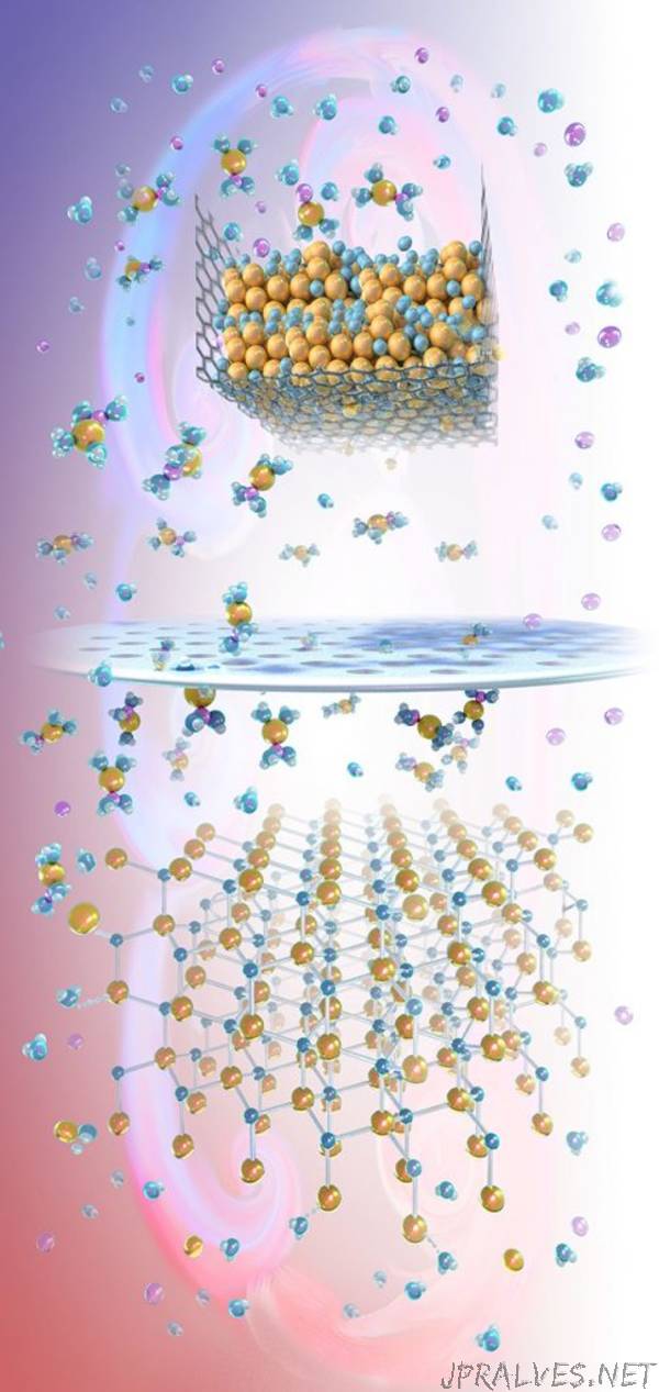
To achieve this higher energy efficiency, a cubic boron nitride (c-BN) single-crystal wafer is needed. Such a wafer could also be used for more efficient high-voltage power electronics due to c-BN’s hardiness. Cubic boron nitride and boron carbide are two of the hardest known materials along with diamond. C-BN is used to drill, cut and ground tough materials into shape. However, the synthesis of c-BN occurs under high-pressure, high-temperature conditions and uses catalysts such as lithium or barium nitride. The temperature is higher than 1,150 centigrade (1423.15 Kelvin) and the process reaches a pressure of 2.5 gigapascals. To realise this higher energy efficient c-BN electronics, a new manufacturing process is needed.
“Under these constraints [of high temperatures and catalysts], synthesis is effectively unscalable, and the process of producing any amount of this material turns out to be enormously expensive and energy intensive,” says Siddha Pimputkar, an assistant professor of materials science and engineering at Lehigh University. Funded with $450,000 and starting on 1 September, last month, Lehigh’s College of Arts and Sciences researchers, including Pimputkar, are aiming to find an easier way to grow single, centimetre-sized crystals of boron nitride.
Boron nitride has been made using chemical vapor deposition, but this cannot produce c-BN in the large quantities of the kind needed for the electronics industry and it produces small crystals. Today, the largest crystal size that can be produced has a diameter of about a millimetre. A solution that is to be investigated is an autoclave system. An autoclave is a heated pressure vessel able to replicate that 2.5 GPa environment.
Pimputkar pursues research focused on enabling and developing advanced materials for use in novel electronic and optoelectronic devices. A method the researchers will investigate to grow the c-BN crystal uses a feedstock of x in a low temperature solution that is fed from below the single crystal seed, which itself is heated. The flow of the feedstock to the crystal through the solution’s motion will grow the crystal.
Pimputkar explains that other possibilities for mass produced c-BN include, more efficient solid-state ultra violet light emitting diodes, lasers for use in disinfecting water, surfaces, and air and sensors for neutron detection. The manufacturing techniques Pimputkar and his colleagues are developing could also be used for producing other materials such as cubic silicon nitride, which is a transparent ceramic that can be used for extremely hard windows. The United States government’s National Science Foundation is also supporting the work.
In 2016, researchers at North Carolina State University announce that they had found a way of making c-BN using high-power laser pulses and quenching, which is a rapid cooling process. Carried out in ambient air pressure, the North Carolina researchers can make a c-BN thin film in about one-fifth of a microsecond with a 500 to 1000 nanometre thick layer of boron nitride (h-BN) that is heated to 2,800 degrees Kelvin with the pulse lasers and then quenched using a substrate heat sink. The quenching time is a significant factor in determining if c-BN is made and not another version of boron nitride.”