
These are the instructions for assembling CSEduino version 2.
Changes
- Changed the position of the voltage regulator
- Changed the orientation of the serial programming pins
- Removed the Pin-13 LED and Jumper
- Less height due to changes in the voltage regulator
- More GND and VCC pins
Bill of Materials
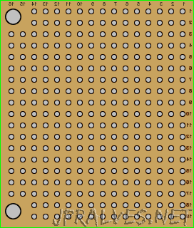
- 1x Stripboard with at least 19 Rows and 16 Columns (€ 0,73)
- 1x ATmega328P-PU microcontroller with Arduino bootloader (U1) (€ 1,59)
- 1x 28 pin DIP IC Socket (U1)
- 1x 16 MHz crystal oscillator (XTAL1) (€ 0,44)
- 2x 22 pF, 50 V ceramic capacitors (C3, C4) (€ 0,06)
- 1x 7805 linear voltage regulator (U2) (€ 0,22)
- 2x 100 μF, 25 V electrolytic capacitors (C1, C2) (€ 0,04)
- 1x 1N4001 rectifier diode (D1) (€ 0,02)
- 1x SPST momentary normally-open type switch (S1) € 0,08)
- 1x 10 kΩ resistor (R2) (€ 0,01)
- 1x 100 nF, 50 V ceramic capacitor (C5) (€ 0,06)
- 1x 1 kΩ resistor (R1) (€ 0,01)
- 1x 40-pin male single header (J1-J7)
The price presented is an average price. All components are very inexpensive except for the Atmega.
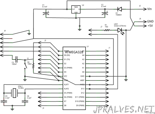
Schematics
Voltage Regulator
To Assemble the voltage regulator part the required components are:
- 1x 7805 linear voltage regulator (U2)
- 2x 100 μF, 25 V electrolytic capacitors (C1, C2)
- 1x 1N4001 rectifier diode (D1)
- 1x 40-pin male single header (J1-J7)
The 1N4001 rectifier diode is used to ensure some protection to the circuit, the two 100µF electrolytic capacitors will smooth the In/Out current. The 7805 is a linear voltage regulator that will convert voltages from 7 and 30 volts to a fixed 5 volts, with a current up to 1 amp.
Notes:
- The 1N4001 (D1) is placed at the front of the +Vin
- One 100µF electrolytic (C2) capacitor sits between +Vin and GND on the 7805 (U2)
- The other 100µF electrolytic (C1) capacitor sits between +Vout and GND on the 7805 (U2)
- You can use a 9V battery to easily power the circuit.
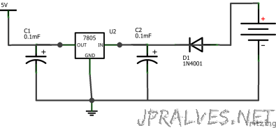
Never power the board with both the battery and the USB programming breakout card.
USB/FTDI Programming Header
To Assemble the USB/FTDI interface part the required components are:
- 1x SPST momentary normally-open type switch (S1)
- 1x 10 kΩ resistor (R2)
- 1x 100 nF, 50 V ceramic capacitor (C5)
- 1x 40-pin male single header (J1-J7)
Notes:
- The 10k ohm resistor (R2) goes between +5v and Pin 1 (RESET) on the ATmega328P Microcontroller
- The SPST switch (S1) goes between GND and Pin 1 (RESET) on the ATmega328P Microcontroller
- The 100nF capacitor (C5) sits between Pin 1 (RESET) on the ATmega328P Microcontroller and FTDI Pin 6 (RTS)
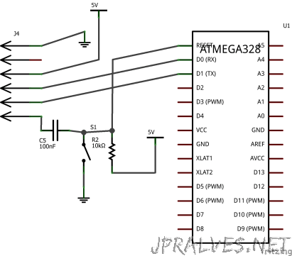
Never power the board with both the battery and the USB programming breakout card.
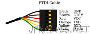
USB/FTDI Pins:
- Pin 1: DTR
- Pin 2: RX
- Pin 3: TX
- Pin 4: VCC
- Pin 5: CTS
- Pin 6: GND
Microcontroller
To Assemble the microprocessor with the headers and external Crystal:
- 1x ATmega328P-PU microcontroller with Arduino bootloader (U1)
- 1x 28 pin DIP IC Socket (U1)
- 1x 16 MHz crystal oscillator (XTAL1)
- 2x 22 pF, 50 V ceramic capacitors (C3, C4)
- 1x 40-pin male single header (J1-J7)
The ATMega328P-PU is a microcontroller. It’s an integrated chip that contains a processor, various types of memory to hold data and binary code and several I/O ports.
Notes:
- Each 22pF capacitor (C3, C4) goes between GND and one of the 16 MHz oscillator pins
- The 16 MHz crystal oscillator (XTAL) connects to Pin 10 and Pin 9 (XTAL2 and XTAL1) on the ATmega328P Microcontroller (U1)
- When looking at the IC in the photo, notice that pin number 1 is at the top-left of the IC and is marked by a small dot.
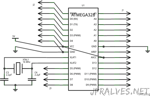
The ATmega328P Pin Layout
The numbering scheme used by Arduino is somewhat different from the Pin numbers of ATmega328P so the following image shows the relation between those numbers:
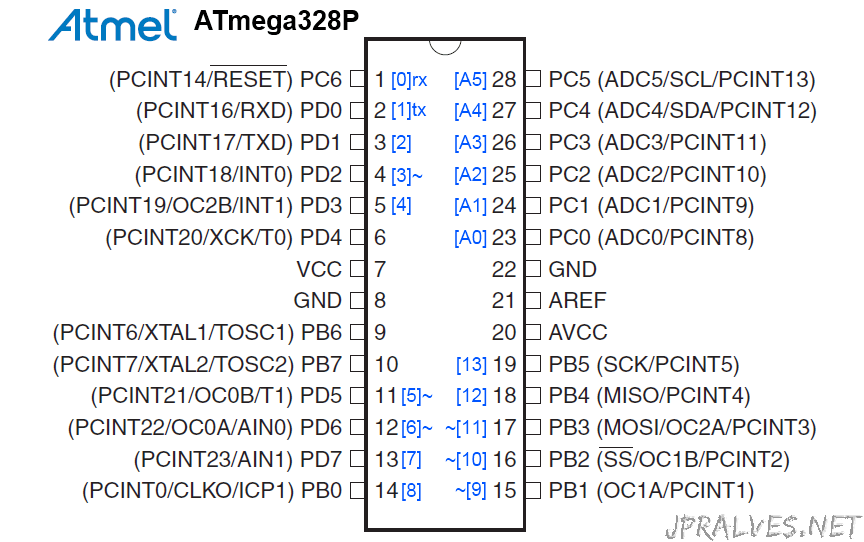
ATmega328P Pins:
- Pin 1: Connect to 10k Resistor -> GND, Connect to Push button -> 100nF capacitor -> Connect to Pin 6 (USB/FTDI)
- Pin 7, 20: VCC (+5V)
- Pin 8, 22: GND
- Pin 9: Connect to 22pF capacitor -> GND, Connect Crystal
- Pin 10: Connect to 22pF capacitor -> GND, Connect Crystal
- Pin 2: Connect to Pin 4 (USB/FTDI)
- Pin 3: Connect to Pin 5 (USB/FTDI)
- Pin 2, 3, 4, 5, 6, 11, 12, 13 ,14, 15, 16, 17, 18: Digital Pins
- Pin 19: Connect to Head -> 1k Resistor -> LED -> GND
- Pin 23, 24, 25, 26 , 27, 28: Analog Pins
- Pin 21 - AREF is not used.
Pins with PWM
- Pins 4, 11, 12, 15, 16 ,17 have PWM.
Assembling the board
Tools required for assembling
- Soldering Iron
- Track Cutter
- Wire Snips
- Solder
Preparing for the Assembly
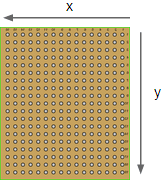
Common stripboards have one side with the “stripes” and another clean side. The components will be mounted on the clean side and soldered on the strip side.
Clean side / Strip Side
Cut holes in the stripboard
Soldering components
Solder the components in the following order:
- Wires
- IC Socket (U1)
- Resistors (R1, R2)
- 1N4001 (D1) - Watch Side
- Ceramic Capacitors (C3, C4, C5)
- Crystal (XTAL)
- SPST switch (S1)
- Male Head Pins (J1, J2, J3, J4, J5, J6, J7)
- Electrolytic Capacitors (C1, C2)
- 7805 (U2)
- ATmega328P (U1)
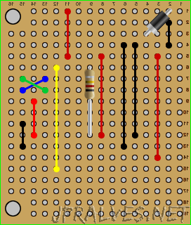
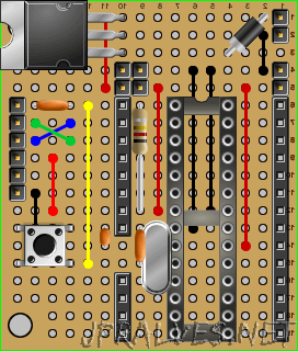
Soldering components location
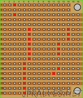
After each component there are coordinates LyCx where y is the line and x is the column to put the wire.
The lines and columns are numbered on the strip side so the x is backwards.
Wires
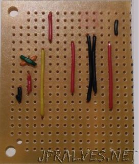
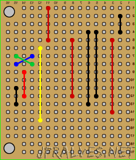
Cut wires with the following lengths:
TODO Corrigir
- Black:
- 2 x 3 cm (L4C3-L12C3, L4C8-L13C8)
- 1 x 1 cm (L2C9-L4C9)
- Red:
- 2 x 3 cm (L5C2-L14C2, L5C6-L12C6)
- 2 x 1 cm (L3C12-L5C12, L5C14-L6C15)
- Green:
- 1 x 3,5 cm (L3C5-L15C5)
- Yellow:
- 1 x 3 cm (L6C13-L11C16)
Solder the wires into the stripboard according to the image.
Resistors (R1)
The Resistors don’t have polarity but R1 is different from R2.
Solder carefully according to the image.
Components:
- R2 - 10 kO resistor (L6C9 - L12C9) TODO
1N4001 (D1)
Solder the component in the board with the stripe (-) on the left.
Components:
- D1 - 1N4001 rectifier diode (L1C2 - L1C5)
IC Socket (U1)
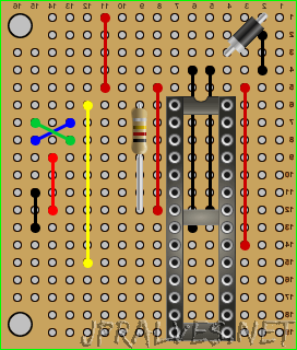
Place the IC Socket with pin 1 on the top.
Its not very easy to solder because the two wires below get in the way. Try to center the wires under the socket.
Solder carefully according to the image.
Components:
- U1 - 28 pin DIP IC Socket (L6C7 - L19C4)
Crystal (XTAL)
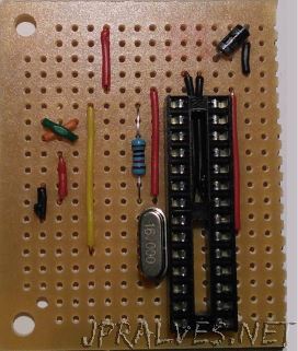
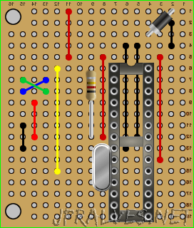
The Crystal doesn’t have polarity. Solder carefully according to the image.
Components:
- XTAL - 16 MHz crystal oscillator (L14C8 - L15C8)
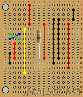
Ceramic Capacitors (C3, C4, C5)
The Ceramic Capacitors don’t have polarity but C5 is different from C3 and C4. Solder carefully according to the image.
Components:
- C3 - 22 pF, 50 V ceramic capacitor (L13C11 - L15C11)
- C4 - 22 pF, 50 V ceramic capacitor (L13C9 - L14C9)
- C5 - 100 nF, 50 V ceramic capacitor (L9C15 - L11C15)
SPST switch (S1)
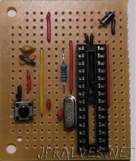
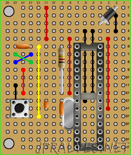
To solder this component you should straighten the pins so it fits in a 3 x 3 space. Solder carefully according to the image.
Components:
- S1 - SPST normally-open type switch (L11C14 - L13C12)
7805 (U2)
The metal side should be facing right and letters on the chip should be facing left. Solder according to the image.
Components:
- U2 - 7805 linear voltage regulator (L1C10-L3C10)
Male Head Pins (J1, J2, J3, J4, J5, J6, J7)
These should be soldered carefully. Solder only one pin at the beginning so its easier to straighten the head, then solder the rest.
Solder carefully according to the image.
- J1 - 1x14-pin male header (L6C1-L19C1)
- J2 - 1x8-pin male header (L6C10-L13C10)
- J3 - 1x4-pin male header (L16C10-L19C10)
- J4 - 1x6-pin male header (L4C16-L9C16)
- J5+J6 - 1x5-pin male header* (L1C1-L5C1)
J7 - 1x2-pin male header (L2C6-L3C6)
- Remove 2 of the pins.
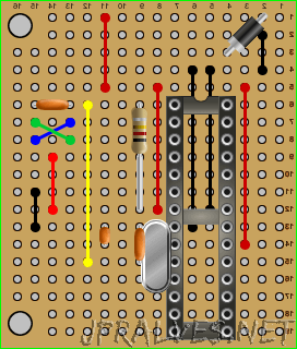
Electrolytic Capacitors (C1, C2)
The C1 should have the (-) side up and the (+) side down. The minus is normally identified by a white strip and shorter leg.
The C2 should have the (-) side down and the (+) side up.
Solder according to the image.
Components:
- C1 - 100 µF 25 V electrolytic capacitor (L2C13- - L2C13+)
- C2 - 100 µF 25 V electrolytic capacitor (L1C8+ - L2C8-)
ATmega328P (U1)
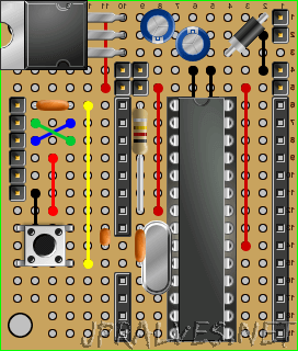
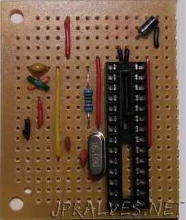
Then, after finishing you can put the ATmega328P on the socket according to the image.
Components:
- U1 - ATmega328P-PU microcontroller
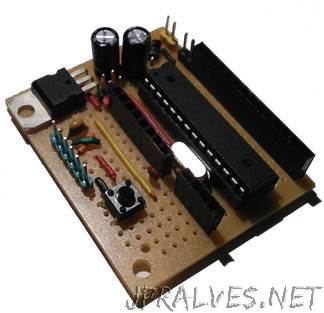
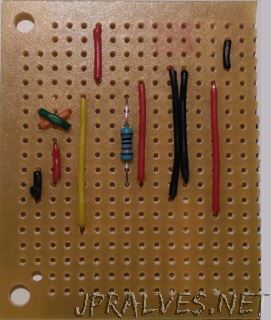
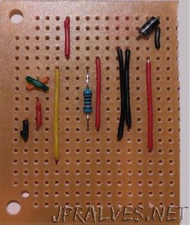
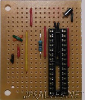
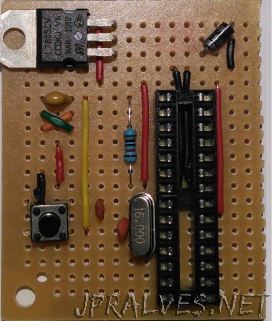
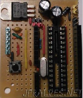
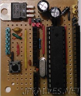
The fully assembled board will look like this:
Running a Test Sketch
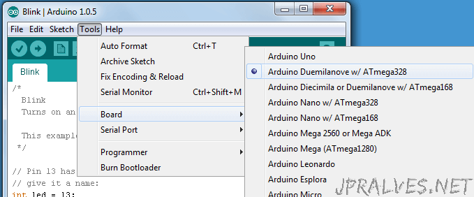
Open Arduino IDE. Select The proper hardware - Menu Tools -> Board -> Arduino Duemilanove w/ ATmega328.
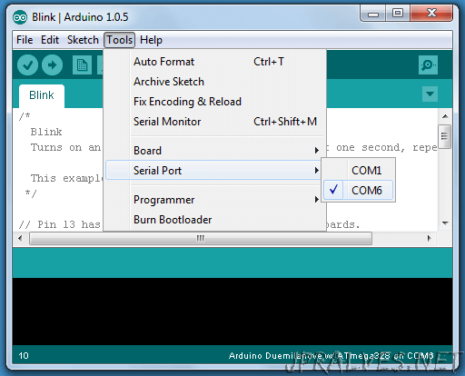
Select the correct Serial Port after connecting the FTDI Breakout board In the Menu Tools -> Serial Port.
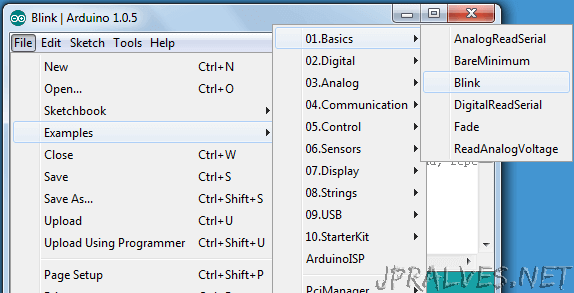
Without adding anything else you can run the following sketch (Menu File -> Examples -> 01. Basics -> Blink):
/*
  Blink
  Turns on an LED on for one second, then off for one second, repeatedly.
  This example code is in the public domain.
 */
// Pin 13 has an LED connected on most Arduino boards.
// give it a name:
int  led = 13;
// the setup routine runs once when you press reset:
void  setup () {
  // initialize the digital pin as an output.
 pinMode (led, OUTPUT );
}
// the loop routine runs over and over again forever:
void  loop () {
  digitalWrite (led, HIGH ); // turn the LED on (HIGH is the voltage level)
  delay (1000); // wait for a second
  digitalWrite (led, LOW ); // turn the LED off by making the voltage LOW
  delay (1000);               // wait for a second
}
After Uploading (Ctrl-U) the program should start afterwards.
The LED on the board should blink every second.
Note: Do not connect the external power to the board when using the USB/FTDI programming breakout card.