
“Harnessing the sun’s rays to produce solar power is an expanding industry with positive environmental impacts. As sunlight reaches semiconducting materials, it is converted into electricity through a photovoltaic system of solar cells, generating renewable, clean energy that can run everything from small electronic devices to electric lighting to race cars. One growing area in solar power research is perovskite materials, which have a unique structure that makes possible low-cost, efficient photovoltaic cells used to convert the harvested solar energy into useful electricity for homes, businesses, and military.
These perovskite solar cells, or PSCs, are one of the fastest developing solar technologies, with broad applications due to their unique optical and electronic properties. PSCs combine organic and inorganic materials, and can be built using low-cost manufacturing methods, making production inexpensive and efficient.
Despite these advantages, PSC materials have some limiting characteristics. Their stability is very poor, causing them to perform well for a few hours or days, and then decay quickly. And many PSCs contain lead-based material as the light-harvesting active layer, restricting their usability in wearable electronic devices.
Purdue University scientists and engineers have created a new set of perovskite materials that combine the hydrophobic qualities of the existing organic materials, which make the materials stable, with a series of new organic building blocks introduced into the perovskite that contain their own semiconducting functionalities. The team recently published two papers detailing their discoveries in new perovskite compositions and applications.
The first study, in the latest issue of Nature Chemistry, demonstrates how the researchers from Purdue University, ShanghaiTech University, Duke University, and Lawrence Berkeley National Laboratory controlled the interaction between the organic molecules and perovskites to form a series of new hybrid structures. The team came up with a molecule design strategy to reduce the self-aggregation or interaction between the organic molecules themselves, guiding how the organic molecules fit into the inorganic structure and improve the properties of the perovskites.
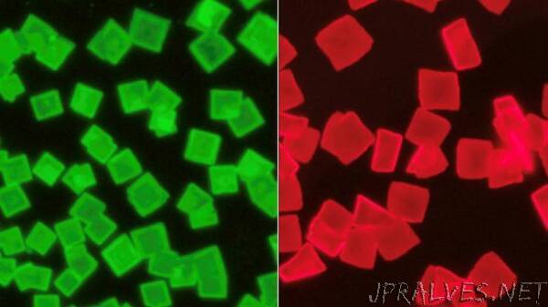
Typically, the organic and inorganic materials do not “want” to bond together. The organic side of the materials is softer, and the inorganic side is more rigid, causing the organic material to constantly move. Since the materials are not fixed, it is more difficult to accurately determine the position of the organic material. It took the researchers several attempts to find the right method to grow single crystals, which allowed them to determine the best crystal structure – similar to a “sandwich,” with inorganic materials held between layers of organic molecules on either side.
“These structures are very exciting. The sandwich structures are like the GaN or GaAs semiconductor quantum wells that are widely used today in many electronic and optoelectronic devices, but they are much easier to produce and more tolerant to defects,” said Letian Dou, Assistant Professor in the Davidson School of Chemical Engineering at Purdue University, who led the research team.
“This began the foundation for a variety of electronic device applications, and broadened our understanding of optical and electronic properties and materials stabilities,” said Libai Huang, Associate Professor in the Department of Chemistry at Purdue University.
The beginning research resulted to the team’s second study, featured in the September 2019 Journal of the American Chemical Society, which took the organic-inorganic hybrid perovskite materials and demonstrated their increased stability and performance in a field effect transistor (FET), an electronic device that uses an electric field to control the flow of current. FETs are used in integrated circuits in devices such as computers and wireless communications. It is noted that the new materials do not contain toxic element Pb, making this technology more environmentally friendly and practically sound.
The potential uses for this type of material are very broad because semiconductors are the foundation of essentially all electronic and optoelectronic devices like transistors, solar cells, LEDs, and photodetectors key parts in computers, televisions, and cameras. The new organic-inorganic hybrid perovskite materials are cheaper and perform better than a traditional inorganic semiconductor. And the new materials design strategy could serve as a blueprint for many other functional hybrid materials.
“Solar cells, as many people have demonstrated, can be highly efficient,” noted Yao Gao, the lead author of both works and a postdoctoral fellow in Dou’s research group. “With our new technology, we can make the hybrid perovskite materials intrinsically more stable. By replacing the toxic lead, these new materials are better for the environment, and can also be safely used for bioelectronics sensors on the body.”
The organic-inorganic hybrid perovskite materials have the potential to be scaled up for commercial use, the researchers say. The team plans to continue making new crystal structures, enhancing their charge carrier transport properties and stability, which they anticipate will lead to further studies on the chemistry and physics of 2D hybrid perovskite materials.
This research was financially supported by the U.S. Office of Naval Research, Davidson School of Chemical Engineering and College of Engineering at Purdue University.”